


PCB Netlists Explained: How Schematics Connect to Layouts

Quick Answer: A PCB netlist is a machine-readable description of every electrical connection in a circuit. Netlists connect schematic capture to PCB layout by defining how components should be electrically connected throughout the design process.
Key Takeaways
- PCB netlists are automatically generated from a validated schematic, converting every electrical connection into a structured dataset for downstream design tools.
- Imported netlists generate the layout's connectivity (ratsnest) and enable DRC to verify that every routed trace matches the intended electrical design.
- Modern unified EDA platforms like Flux eliminate manual netlist exports by maintaining a live connectivity model that keeps schematics and layouts synchronized automatically.
What Is a PCB Netlist?
A PCB netlist is a plain-text, ASCII-formatted file that excludes every graphical symbol and wire from a schematic to generate a structured list mapping specific component pins to their shared electrical nodes. Schematics function as visual abstractions, using graphic symbols and drawn lines for human readability. Layout engines simply cannot process these images. Consequently, the software demands a strict mathematical map tying every physical component pin directly to its assigned electrical net. Such a netlist provides that mapping and becomes the source of truth for your electronic design automation (EDA) software. When you import one into a layout environment, the tool knows exactly which pad on U1 must connect to which pad on C4, for example, with no ambiguity.
Because different engineering stages require different data structures, several netlist formats exist. The format you export depends on whether you are running a simulation, exchanging data between tools, or testing a bare board.
Common PCB Netlist Formats and Uses
| Format | Primary Use | Description |
|---|---|---|
| SPICE | Circuit Simulation | Defines connections and component values so simulators can calculate voltages and currents at each node. |
| EDIF 2 0 0 | Tool Data Exchange | A vendor-neutral format based on S-expressions used to transfer schematic data between different CAD tools. |
| IPC-D-356 | Bare Board Testing | This standard maps net names and pin connections to physical X/Y coordinates, letting automated test equipment verify bare board continuity before assembly. |
How Netlists Are Generated
Netlist generation requires a clean schematic database. The CAD software parses every schematic file, identifies each node where a wire intersects a component pin, and groups those intersections into named nets. Any two pins sharing a net name get recorded as electrically connected.
The extraction process enforces strict rules before a run. To satisfy such conditions, the design must pass an Electrical Rules Check (ERC), which scans for floating pins, conflicting output drivers, and unconnected nets. Generating a netlist exposes such errors directly. For example, a pin with no assigned net simply cannot be written into the connectivity matrix, so the export fails and forces the designer to fix the schematic capture first.
What Information Does a Netlist Contain?
A standard netlist file contains three data types:
- Reference designators
- Pin numbers
- Net names
The syntax varies by CAD vendor, but the underlying structure is identical across tools. The software names a net and then lists every component pin attached to it.
Below is a Protel-formatted ASCII netlist example:
[
GND
U1-4
C1-2
C2-2
]

[
3V3
U1-8
C1-1
R1-2
]

[
Data_TX
U1-2
R1-1
]
The GND block tells the layout tool to connect pin 4 of U1, pin 2 of C1, and pin 2 of C2 to the same net. If you modify a footprint or change a reference designator during schematic capture, those pin numbers update on the next export. Specialty formats like IPC-D-356 extend this structure by adding physical X/Y coordinates for each test point, which bare board testers use to verify continuity.
How Netlists Drive PCB Layout
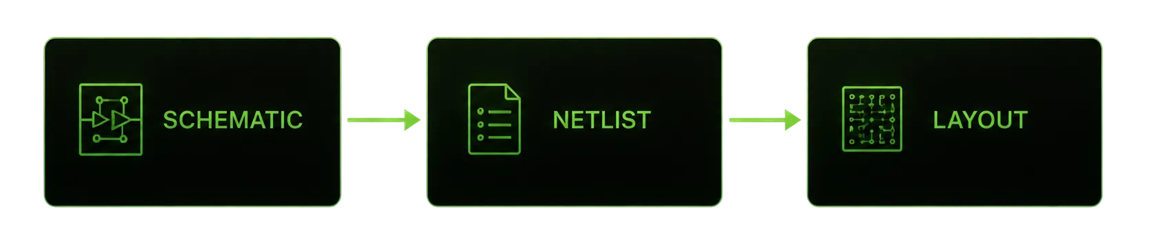
Once the layout software imports the netlist, it projects the logical connections into the physical workspace by generating a ratsnest: a visual web of straight lines connecting component footprints according to associated net assignments. Such lines as part of the ratsnest show you what needs to be routed, not how to route it.
As you route traces, the background Design Rule Checker (DRC) constantly validates your physical copper paths. It measures these real-world routes against the strict logic constraints dictated by the imported netlist file. For example, if you attempt to connect a 3V3 pad to a GND pad, the software triggers a DRC violation and blocks the connection. The netlist acts as a boundary condition on the entire routing process, ensuring the finished copper matches the original schematic intent.
Common Netlist Problems
Layout tools trust the imported netlist without question. As a result, any pin mismatches or missing connections hidden inside that text file will generate physical boards that fail in highly predictable ways.
- Pin mismatches are among the most common causes of scrapped boards. For example, if a MOSFET schematic symbol labels its terminals as pins 1, 2, and 3, but the physical footprint numbers its pads as Gate, Source, and Drain, the netlist generator cannot map the connections. The layout tool will either leave the pads unconnected or assign them incorrectly. Neither of these outcomes are recoverable without a board respin.
- Sync failures are the other major failure mode. Consider the following common scenarios:
- An engineer adds a pull-up resistor to the schematic but forgets to regenerate and re-import the netlist. Because the layout engine stays completely blind to the new part, the physical board goes to manufacturing and ships missing that connection.
- A footprint swap updates pad numbering in the library but not in the cached netlist. Thanks to this oversight, the layout reflects the old mapping.
- Two engineers work on schematic and layout in parallel using separate file exports. Inevitably, their local netlist versions diverge without any warning, causing silent sync errors without triggering a single system warning.
Each scenario produces a board that passes DRC but fails electrically, because the DRC can only check against the netlist it was given.
Modern Netlist Workflows
The legacy workflow -- export an ASCII netlist, open a layout tool, import the file, repeat after every schematic change -- creates a disconnected snapshot at each export step. Every snapshot is a potential version mismatch. Such sync failures are the predictable consequence of managing connectivity through manual file transfers.
Modern unified EDA environments eliminate manual netlist handling by maintaining connectivity as a live data model. For instance, Flux uses a connected schematic-to-layout architecture where drawing a wire on the schematic immediately updates the ratsnest in the layout. There is no export step, no file to import, and no version to track. Rather, the netlist exists as a continuous internal state rather than a periodic file artifact, which closes the gap where those synchronization errors originate.
Ready to stop managing manual file exports and dealing with disconnected sync failures? Flux's cloud-native, connected architecture eliminates the gap between schematic and layout by maintaining a live PCB netlist that updates instantly as you design. Start your next project in Flux today and experience a modern, seamlessly integrated hardware workflow.
More in PCB Design & Engineering Fundamentals

What Is a PCB? A Beginner's Guide to Printed Circuit Board Design

What is Schematic Design? All You Need to Know

PCB Stackup Design: How to Build the Right Layer Structure

Best PCB Routing Techniques for Clean Circuit Board Layouts

How to Read PCB Schematics: A Beginner-Friendly Guide

PCB Schematic Best Practices for Clean Circuit Design

Schematic Capture Explained: How Engineers Create Circuit Diagrams

Common Schematic Design Mistakes and How to Avoid Them

What Is a Netlist? Understanding the Basics of Electronic Design Automation

PCB Symbol Design: Best Practices for Clean Schematics

Making Parts Just Got Easier: Introducing Parametric Symbols

Create Satisfying Schematics with these Updates

Electronic Circuit Design Explained: From Schematics to PCB Layout

Designing PCBs: What Are the Essential Steps

Hardware Design Workflow: From Schematic Capture to Manufacturing

What Is a Functional Block Diagram and Why Is It Critical in System Design

PCB Design Basics: What You Need to Know Before You Start

Diode Symbols: How to Identify Common Diodes

Ultra Librarian joins Flux to Take the Hard out of Hardware

Flux Now Has the World's Largest eCAD Part Library

Capacitor Symbols Explained: Types, Polarity, and Schematic Use

MOSFET and Transistor Symbols Explained: NMOS, PMOS, NPN, and PNP

How to Convert PDF Schematics into Editable EDA Files Using AI

Crosstalk, Reflections, and the Real Challenges of Signal Integrity

What Is Signal Integrity in PCB Design? A Practical Guide

High-Speed PCB Design: Layout Rules, Signal Integrity, and Routing Best Practices

EMI/EMC in PCB Design: How to Reduce Interference

PCB EMI Problems: Causes and Solutions

Differential Pair Routing Guidelines and Controlled Impedance Best Practices

PCB Impedance Control: A Practical Guide for Engineers

Introducing Curved Traces in Flux

Analog vs Digital PCB Design: Key Differences Explained

Pi Filters Explained: Design, Components & Applications

RS485 Explained: Wiring, Specifications, and Applications

What is RS232?

SPI vs. I2C: Which Communication Protocol Should You Use?

RJ45 Connectors: Pinouts, Categories, Uses, and Testing

CO2 Sensor Technology: How These Devices Detect Carbon Dioxide

Hall Effect Joysticks: How They Work, Benefits, and Uses

What Is an Oscillator? Beginner's Guide to Oscillating Circuits

Flexible PCB Design Guide: Materials, Layout, and Applications

Rigid-Flex PCB Design: Benefits, Challenges, and Layout Tips

The RF Engineer's Guide to Designing Printed Trace Antennas

SMA Connectors Explained: Types, Applications, and PCB Design Considerations

RC Low-Pass Filter: Formula, Cutoff Frequency & Design

Decoding Voltage Regulators: How They Work in Everyday Electronics

Voltage Regulators: How They Work, Types, and Applications

Buck Converter Design: Components, PCB Layout, and Formulas

Buck and Boost Converters: How They Work and Where They’re Used

LM2596 in Action: Case Study of Its Application in Power Supply Units

Guide to GND Fills and Power Planes

Power Distribution Network (PDN) Design in PCBs

PCB Grounding Techniques for Noise Reduction and Stability

Designing High-Current PCBs: Layout and Safety Considerations

How to Calculate PCB Trace Resistance

Voltage Drop Calculations: Formulas, Factors, and Guidelines

AC to DC Converter: The Backbone of Power Electronics

AC-to-DC Converters: How They Work, Types, and Design Tips

Thermal Management in PCB Design: Methods and Best Practices

PCB Thermal Management: Analysis and Design Best Practices

Understanding PPS Fast Charging: What It Is and How It Works

Decoupling Capacitors in PCB Design: Placement and Selection

What Is a Multilayer Ceramic Capacitor (MLCC)?

Tantalum Capacitors Guide: Polarity, Derating & Risks

Amps vs. Volts: Key Differences and How They Work Together

Never Worry About Stackups Again: Introducing the Stackup Editor

Multilayer PCB Design: Best Practices for Circuit Board Layout

How to Choose PCB Materials: FR4 vs Advanced Substrates

Blind Vias, Buried Vias, and Microvias: A Complete Guide to PCB Via Types

Exploring Different Types of Vias in PCB

High-Density PCBs just got easier with Smart Vias

How to Use Via Stitching in PCB Design

PCB Design Constraints: What Engineers Need to Know

PCB Constraint Management: How Engineers Control Layout Rules

Design Rule Checking (DRC) in PCB Design: Real-Time vs Batch, Rules, and Common Failures

Electrical Rule Check (ERC) vs DRC in PCB Design

PCB Design Reviews: Best Practices for Catching Errors Early

Common PCB Design Mistakes and How to Avoid Them

5 Common PCB Design Mistakes and How to Avoid Them

PCB Silkscreen Design: Guidelines and Common Mistakes

Smart Polygons: Advanced PCB Design Just Got Easier

Automatically Create Photorealistic PCB Renders

How to Convert from MM to Mils: a Guide for Beginners

What Is Solder Mask? Materials, Colors, and PCB Design Rules

Designing Custom PCB Outlines: Fixing DXF and SVG Import Failures

PCB Enclosure Design: How to Design an Enclosure

Component Selection in PCB Design: How Engineers Choose the Right Parts

Smarter Part Search Just Got a Major Upgrade

How to Design a PCB Footprint (Step-by-Step Guide)

Protection Circuit 101: Securing Your Electronics from Overcurrent and Short Circuits

Understanding the Flyback Diode: Your Essential Guide to Functionality and Why You Need One

What Is a Zener Diode? How It Works and Where It’s Used

Understanding the Fundamentals: MOSFET Basics for Beginners

LM741 Pinout: A Deep Dive into a Classic Op Amp

6 Types of Variable Resistors: a Detailed Look at Their Uses
Parallel and Series Resistor Calculator

Resistor Color Code Calculator

SMT vs Through-Hole Technology: Which Should You Use?

How to Use Flux When Soldering Electronics

The Ultimate Guide to Toggle Switches: Types, Uses, and How They Work

What Is the Science Behind Push Button Switches and How They Work

Tactile Switches: Wiring, Debouncing, and PCB Design

Electrical Wire Connector Types and Uses

Why Your PCB Is Failing: Debugging Common Issues

555 Timer Guide: Pinout, Operating Modes, and Circuit Examples

Inverting Op-Amp Circuits: Formula, Gain, and Design Examples

How to Wire a Potentiometer: Pinout, Diagrams, and PCB Examples
Let’s start building.

Let’s build your idea together. All you need to do is describe what you want to make, or what problem you want to solve. Flux will work with you to make it a reality.
