


Differential Pair Routing Guidelines and Controlled Impedance Best Practices

As data rates increase, single-ended signals become more sensitive to noise, timing errors, and electromagnetic interference. Hardware engineers therefore use differential signaling for interfaces such as USB, HDMI, PCIe, Ethernet, and other high-speed buses. Proper differential pair routing helps maintain controlled impedance, limit timing skew, reduce noise susceptibility, and preserve signal integrity across the PCB.
Key Takeaways
- Maintaining consistent trace width and spacing helps preserve controlled impedance during differential pair routing.
- Precise length matching PCB practices minimize intra-pair skew so both signals reach the receiver within the interface's timing tolerance.
- Proper high speed routing uses continuous reference planes, controlled geometry, and adequate clearance from nearby signals to reduce reflections, crosstalk, and signal degradation.
What Are Differential Pairs?
Modern PCB differential pairs consist of two traces carrying complementary electrical signals. The transmitter drives the two lines with opposite voltage changes, while the receiver measures the voltage difference between them. Because the receiver responds primarily to the difference between the two signals, differential signaling can reject noise that couples similarly onto both traces.
The effectiveness of such common-mode noise rejection depends on maintaining electrical and geometric balance throughout the pair. Differential pairs are commonly identified as positive and negative signals, such as D+ and D-, TX+ and TX-, or P and N.
Why Differential Pair Routing Matters
Accurate PCB routing helps high-speed interfaces stay within their electrical limits. Protocols such as USB, HDMI, PCIe, and Ethernet depend on several routing characteristics working together:
- Differential impedance: The pair must stay close to the target impedance defined by the interface and PCB stackup.
- Intra-pair skew: Excessive length difference between the positive and negative traces can distort the differential signal.
- Crosstalk: Nearby high-speed traces can couple unwanted energy into one or both members of the pair.
- Return-path continuity: Splits or voids in the reference structure can disturb the electromagnetic environment around the traces.
- Via and connector transitions: Pads, vias, and connectors can introduce local impedance discontinuities.
Poor differential signal routing techniques can therefore create reflections, timing errors, mode conversion, and electromagnetic interference. Good signal integrity PCB practices help preserve enough voltage and timing margin for the receiver to interpret the signal reliably.
Key Differential Pair Routing Rules
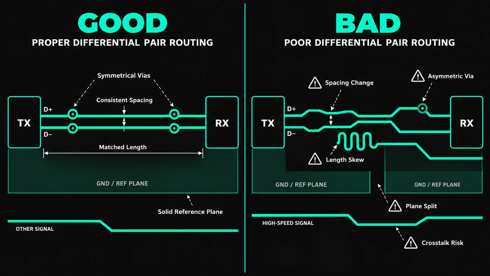
Designers should control the pair's geometry from the transmitter to the receiver as consistently as the PCB layout allows. Trace width, spacing, reference-plane continuity, and electrical length all contribute to how the pair behaves at high frequencies.
Keep the Pair Coupled
Route the positive and negative traces together and maintain consistent spacing for as much of the route as practical. Temporary separation may be unavoidable near component pins, connectors, vias, or dense BGA breakouts, but such discontinuities should remain short and the geometry of both traces should be as symmetrical as possible.
Large changes in spacing alter the electromagnetic coupling between the two traces and can change the differential impedance. Restoring the intended spacing quickly after an unavoidable breakout or transition helps limit such discontinuities.
Maintain Consistent Spacing
The spacing between the two traces contributes directly to the pair's differential impedance, but spacing alone does not determine impedance. Impedance matching PCB calculations also depend on trace width, copper thickness, dielectric thickness, dielectric constant, distance to the reference plane, PCB stackup, and whether the traces use microstrip or stripline geometry.
Designers should calculate the required trace geometry against the actual fabrication stackup rather than selecting trace width and spacing independently. Abrupt changes in spacing or trace width create impedance discontinuities that can reflect part of the transmitted signal.
Keep Trace Width Consistent
Maintain the calculated trace width throughout the route wherever possible. Neck-down regions near pads, vias, or fine-pitch components may be unavoidable, but such sections should be kept short and applied symmetrically to both members of the pair.
Keeping both traces geometrically similar helps preserve electrical balance. Significant differences in trace width between the positive and negative sides can introduce impedance imbalance and unwanted common-mode energy.
Control Intra-Pair Length Matching
Proper length matching PCB design focuses first on minimizing the difference in electrical length between the positive and negative traces. A difference in trace length produces intra-pair skew, meaning one side of the differential signal reaches the receiver earlier than the other.
Rather than requiring both traces to arrive at the exact same instant, designers should keep the skew within the tolerance specified by the applicable interface. Matching the total length of one differential pair to another pair or related signal is a separate requirement and depends on the protocol.
Use a Continuous Reference Plane
Route high-speed differential pairs over a continuous reference plane whenever possible. Avoid routing across ground-plane splits, large voids, power-plane boundaries, or gaps created by cutouts and antipads.
Although differential currents largely interact with each other, each trace also couples to the surrounding reference structure. Discontinuities beneath the pair can alter impedance, disturb current return paths, and increase electromagnetic radiation.
Keep Differential Pairs Away From Other Signals
Differential traces should remain close enough to preserve the intended pair coupling while maintaining adequate clearance from unrelated high-speed traces. Routing another signal too close to only one side of the pair can create asymmetric coupling and introduce crosstalk.
The required separation depends on the signal speed, stackup, trace geometry, and applicable design rules. Designers should follow interface-specific or PCB design constraints rather than relying on a single universal clearance value.
Use Symmetrical Via Transitions
Layer changes may require vias, but the positive and negative traces should use matching via structures. Via diameter, drill diameter, pad size, antipad geometry, stub length, and the number of vias should remain as similar as possible for both traces.
Nearby ground stitching vias may also be needed when the reference plane changes between layers. These vias give the return current a short, low-inductance path between the two reference planes, helping minimize the impedance discontinuity caused by the layer transition.
Avoid Excessive Meandering
Length-matching bends or serpentine sections can compensate for local length differences, but they should be used carefully. Place the correction reasonably close to the point where the mismatch occurs and avoid packing adjacent meander segments too tightly.
Closely spaced serpentine segments can couple to one another, changing the effective electrical delay and degrading signal integrity. Gentle bends with adequate spacing are preferable to tightly compressed accordion patterns.
Common Challenges and Mistakes in Differential Routing
Navigating vias, connectors, package escapes, and dense component placement can make it difficult to preserve ideal differential geometry. These constraints often force temporary changes in spacing, width, or layer assignment, so the goal is to keep each transition short and electrically balanced.
Differential Pair Routing Challenges and Solutions
| Challenge | Impact | Solution |
|---|---|---|
| Component Obstacles | Forces the two traces to separate or change direction. | Route both traces around the obstacle using symmetrical geometry and restore the calculated spacing quickly. |
| Layer Transitions | Vias introduce parasitic inductance and capacitance that can disturb impedance. | Use matching vias for both traces, minimize unnecessary transitions, and add nearby ground stitching vias where required. |
| Dense Breakouts | Fine-pitch pads or BGA escapes may require temporary changes in width or spacing. | Keep P/N breakout geometry symmetrical and return to the controlled differential geometry as soon as practical. |
| Connectors and Pads | Pad geometry can create local impedance discontinuities. | Keep transitions short and account for connector, pad, and antipad geometry during high-speed analysis. |
| Length Mismatch | Produces intra-pair skew and differential-to-common-mode conversion. | Correct the mismatch with appropriately spaced tuning structures near the source of the mismatch. |
Common Mistakes in Differential Pair Routing
Most routing failures come from a few repeatable layout errors rather than one single mistake. Watch for the following problems during placement and routing:
- Focusing only on length matching: Equal trace lengths do not guarantee good performance if spacing, width, or impedance changes repeatedly along the route.
- Crossing reference-plane splits: Ground or power-plane voids change the electromagnetic environment and can increase reflections and radiation.
- Routing other signals too close: A nearby trace can couple more strongly to one side of the pair and create asymmetric crosstalk.
- Overusing serpentine tuning: Tightly packed meanders can couple to themselves, so added physical length does not always translate directly into the expected electrical delay.
- Using generic width and spacing values: Controlled impedance depends on the actual PCB stackup, dielectric properties, copper thickness, and reference-plane geometry.
Checking these issues together is more effective than treating differential routing as a length-matching exercise alone. The pair should remain electrically balanced throughout the complete path, including breakouts, vias, connectors, and tuned sections.
Differential Pair Routing Best Practices Checklist
Use the following checklist when routing high-speed differential signals:
How Modern PCB Tools Help Differential Pair Routing
Modern PCB layout tools help designers enforce differential pair constraints throughout the routing process. Depending on the platform, designers may be able to define and check rules for differential pair assignment, trace width, pair spacing, length matching, clearance, via geometry, layer usage, and other routing constraints.
Flux provides a collaborative browser-based PCB design environment where teams can work on schematics and PCB layouts within a shared project workspace. For high-speed designs, automated design-rule checks and clearly defined routing constraints can help identify geometry violations before manufacturing, while final impedance values and interface-specific tolerances should still be verified against the selected PCB stackup. Try Flux to design PCB layouts in a collaborative browser-based environment and apply consistent routing constraints throughout your differential pair routing workflow.
FAQs
Differential pair routing is the process of laying out two electrically related PCB traces that carry complementary signals while controlling their spacing, impedance, geometry, and timing relationship. The goal is to maintain electrical balance between the two traces throughout the signal path.
Length matching minimizes the electrical delay difference between the positive and negative traces. Keeping intra-pair skew within the interface's specified tolerance helps preserve the differential waveform and reduces the amount of differential energy converted into common-mode noise.
Differential impedance depends on several PCB parameters, including trace width, spacing between the traces, copper thickness, dielectric thickness, dielectric constant, distance to the reference plane, and the overall PCB stackup. The required geometry should therefore be calculated using the actual fabrication stackup.
The traces should remain coupled and consistently spaced for as much of the route as practical. Short deviations may be necessary near vias, connectors, pads, and package breakouts, but the geometry should remain as symmetrical as possible and return to the intended routing geometry quickly.
Yes. Vias are acceptable when layer changes are necessary, but both traces should use matching via structures and similar transition geometry. Unnecessary transitions should be avoided because vias introduce parasitic inductance and capacitance that can disturb impedance.
A continuous reference plane is preferred for high-speed differential routing because it provides a consistent electromagnetic environment along the route. Designers should avoid crossing splits, voids, or abrupt changes in the reference structure whenever possible.
There is no universal spacing value for every differential pair. The required spacing depends on the target differential impedance, trace width, PCB stackup, dielectric properties, copper thickness, and the interface specification.
Intra-pair skew is the propagation-delay difference between the positive and negative traces of a differential pair. Excessive skew reduces signal balance, distorts the received waveform, and can convert part of the differential signal into common-mode noise.
More in PCB Design & Engineering Fundamentals

What Is a PCB? A Beginner's Guide to Printed Circuit Board Design

What is Schematic Design? All You Need to Know

PCB Stackup Design: How to Build the Right Layer Structure

Best PCB Routing Techniques for Clean Circuit Board Layouts

How to Read PCB Schematics: A Beginner-Friendly Guide

PCB Schematic Best Practices for Clean Circuit Design

Schematic Capture Explained: How Engineers Create Circuit Diagrams

Common Schematic Design Mistakes and How to Avoid Them

PCB Netlists Explained: How Schematics Connect to Layouts

What Is a Netlist? Understanding the Basics of Electronic Design Automation

PCB Symbol Design: Best Practices for Clean Schematics

Making Parts Just Got Easier: Introducing Parametric Symbols

Create Satisfying Schematics with these Updates

Electronic Circuit Design Explained: From Schematics to PCB Layout

Designing PCBs: What Are the Essential Steps

Hardware Design Workflow: From Schematic Capture to Manufacturing

What Is a Functional Block Diagram and Why Is It Critical in System Design

PCB Design Basics: What You Need to Know Before You Start

Diode Symbols: How to Identify Common Diodes

Ultra Librarian joins Flux to Take the Hard out of Hardware

Flux Now Has the World's Largest eCAD Part Library

Capacitor Symbols Explained: Types, Polarity, and Schematic Use

MOSFET and Transistor Symbols Explained: NMOS, PMOS, NPN, and PNP

How to Convert PDF Schematics into Editable EDA Files Using AI

Crosstalk, Reflections, and the Real Challenges of Signal Integrity

What Is Signal Integrity in PCB Design? A Practical Guide

High-Speed PCB Design: Layout Rules, Signal Integrity, and Routing Best Practices

EMI/EMC in PCB Design: How to Reduce Interference

PCB EMI Problems: Causes and Solutions

PCB Impedance Control: A Practical Guide for Engineers

Introducing Curved Traces in Flux

Analog vs Digital PCB Design: Key Differences Explained

Pi Filters Explained: Design, Components & Applications

RS485 Explained: Wiring, Specifications, and Applications

What is RS232?

SPI vs. I2C: Which Communication Protocol Should You Use?

RJ45 Connectors: Pinouts, Categories, Uses, and Testing

CO2 Sensor Technology: How These Devices Detect Carbon Dioxide

Hall Effect Joysticks: How They Work, Benefits, and Uses

What Is an Oscillator? Beginner's Guide to Oscillating Circuits

Flexible PCB Design Guide: Materials, Layout, and Applications

Rigid-Flex PCB Design: Benefits, Challenges, and Layout Tips

The RF Engineer's Guide to Designing Printed Trace Antennas

SMA Connectors Explained: Types, Applications, and PCB Design Considerations

RC Low-Pass Filter: Formula, Cutoff Frequency & Design

Decoding Voltage Regulators: How They Work in Everyday Electronics

Voltage Regulators: How They Work, Types, and Applications

Buck Converter Design: Components, PCB Layout, and Formulas

Buck and Boost Converters: How They Work and Where They’re Used

LM2596 in Action: Case Study of Its Application in Power Supply Units

Guide to GND Fills and Power Planes

Power Distribution Network (PDN) Design in PCBs

PCB Grounding Techniques for Noise Reduction and Stability

Designing High-Current PCBs: Layout and Safety Considerations

How to Calculate PCB Trace Resistance

Voltage Drop Calculations: Formulas, Factors, and Guidelines

AC to DC Converter: The Backbone of Power Electronics

AC-to-DC Converters: How They Work, Types, and Design Tips

Thermal Management in PCB Design: Methods and Best Practices

PCB Thermal Management: Analysis and Design Best Practices

Understanding PPS Fast Charging: What It Is and How It Works

Decoupling Capacitors in PCB Design: Placement and Selection

What Is a Multilayer Ceramic Capacitor (MLCC)?

Tantalum Capacitors Guide: Polarity, Derating & Risks

Amps vs. Volts: Key Differences and How They Work Together

Never Worry About Stackups Again: Introducing the Stackup Editor

Multilayer PCB Design: Best Practices for Circuit Board Layout

How to Choose PCB Materials: FR4 vs Advanced Substrates

Blind Vias, Buried Vias, and Microvias: A Complete Guide to PCB Via Types

Exploring Different Types of Vias in PCB

High-Density PCBs just got easier with Smart Vias

How to Use Via Stitching in PCB Design

PCB Design Constraints: What Engineers Need to Know

PCB Constraint Management: How Engineers Control Layout Rules

Design Rule Checking (DRC) in PCB Design: Real-Time vs Batch, Rules, and Common Failures

Electrical Rule Check (ERC) vs DRC in PCB Design

PCB Design Reviews: Best Practices for Catching Errors Early

Common PCB Design Mistakes and How to Avoid Them

5 Common PCB Design Mistakes and How to Avoid Them

PCB Silkscreen Design: Guidelines and Common Mistakes

Smart Polygons: Advanced PCB Design Just Got Easier

Automatically Create Photorealistic PCB Renders

How to Convert from MM to Mils: a Guide for Beginners

What Is Solder Mask? Materials, Colors, and PCB Design Rules

Designing Custom PCB Outlines: Fixing DXF and SVG Import Failures

PCB Enclosure Design: How to Design an Enclosure

Component Selection in PCB Design: How Engineers Choose the Right Parts

Smarter Part Search Just Got a Major Upgrade

How to Design a PCB Footprint (Step-by-Step Guide)

Protection Circuit 101: Securing Your Electronics from Overcurrent and Short Circuits

Understanding the Flyback Diode: Your Essential Guide to Functionality and Why You Need One

What Is a Zener Diode? How It Works and Where It’s Used

Understanding the Fundamentals: MOSFET Basics for Beginners

LM741 Pinout: A Deep Dive into a Classic Op Amp

6 Types of Variable Resistors: a Detailed Look at Their Uses
Parallel and Series Resistor Calculator

Resistor Color Code Calculator

SMT vs Through-Hole Technology: Which Should You Use?

How to Use Flux When Soldering Electronics

The Ultimate Guide to Toggle Switches: Types, Uses, and How They Work

What Is the Science Behind Push Button Switches and How They Work

Tactile Switches: Wiring, Debouncing, and PCB Design

Electrical Wire Connector Types and Uses

Why Your PCB Is Failing: Debugging Common Issues

555 Timer Guide: Pinout, Operating Modes, and Circuit Examples

Inverting Op-Amp Circuits: Formula, Gain, and Design Examples

How to Wire a Potentiometer: Pinout, Diagrams, and PCB Examples
Let’s start building.

Let’s build your idea together. All you need to do is describe what you want to make, or what problem you want to solve. Flux will work with you to make it a reality.
