March 21, 2026
What Is a PCB? A Beginner's Guide to Printed Circuit Board Design
Share

Open almost any electronic device, from a basic LED flashlight to a commercial aircraft's avionics bay, and you'll find a printed circuit board (PCB). Before PCBs became the industry standard, electronics were built using point-to-point wiring: Individual wires were soldered directly between chassis-mounted components. This approach made assemblies bulky, prone to error, and practically impossible to mass-produce. The PCB replaced all of that with a single, repeatable, manufacturable structure.
The global PCB market was valued at $67.9 billion in 2023 and is projected to grow to $92.4 billion by 2029. For students learning circuit design or hardware founders building their first prototype, answering the question of what is a pcb—and understanding how it works—is the first step toward moving a concept off the breadboard and into production.
A Printed Circuit Board (PCB) is a rigid or flexible structure that mechanically supports and electrically connects electronic components using conductive pathways typically etched from copper. The PCB includes a laminated sandwich of conductive and insulating materials. During manufacturing, factories glue thin sheets of raw copper, known as copper foil, to a non-conductive base layer. They then chemically etch away the excess foil. This process leaves behind specific copper patterns: traces (which act as flat wires) and planes (which are large, solid areas of copper used to distribute power or ground).
A standard rigid PCB has four primary layers:

A printed circuit board acts as the electrical nervous system of a device. Instead of messy bundles of loose wires, the board uses flat copper lines to physically link the pins of different components together. Power and signals must travel across these physical pathways from power supplies to processors, and from sensors to memory, without degrading. Three structural features handle all this electrical traffic:
Traces are the etched copper pathways that carry current from one component to another. When routing these lines, designers manage two main variables: trace width and copper thickness. Trace width dictates how much current the path can safely handle. A power trace delivering 5 amps needs to be substantially wider than a simple data trace toggling at 3.3 volts. Copper thickness is measured in ounces (oz) per square foot, with 1 oz or 2 oz copper being common standards. If you size a power trace too narrow or use copper that is too thin, the electrical resistance increases. This generates excess heat and causes a voltage drop that can reset your processor mid-operation.
Pads are small, exposed copper areas, free of the green solder mask, where parts attach to the board. This is where you solder component leads (the long metal wire legs found on traditional through-hole parts) or surface-mount terminals (the flat metal contacts built onto the bodies of modern, low-profile chips). Every resistor, integrated circuit, and connector lands on a pad.
Vias solve the problem of routing signals across multiple layers. Vias are metal-lined drilled holes that enable electrical interconnections between conductive layers, essentially a copper-plated tunnel connecting a trace on layer 1 to a trace on layer 4, or any other layer combination.
A bare board with etched copper pathways does nothing on its own; it is essentially a blank canvas waiting for parts. It only becomes functional once you solder active and passive components onto those exposed pads. In manufacturing terminology, the bare board is the PCB; once populated with parts, it becomes a Printed Circuit Board Assembly (PCBA).
The components you choose dictate what the circuit does:
Designing a printed circuit board follows a sequential engineering workflow. Whether a student is building a first prototype or a hardware startup is pushing a new consumer device to mass production, the core development cycle remains essentially the same.
As circuits grow more complex, routing all connections on a single copper layer becomes geometrically impossible. The solution is adding layers. PCBs can be single-sided (one copper layer), double-sided (two copper layers on both sides of one substrate layer), or multi-layer (stacked layers of substrate with copper sandwiched between).
Beyond layer count, boards split into rigid (standard FR4) and flexible (FPCB). Flexible PCBs are made from flexible materials like polyimide, allowing them to bend and fold to fit into compact and irregular spaces. They show up in folding smartphones, wearable devices, and camera hinges–anywhere a rigid board physically can't go.
Three problems account for the majority of real-world board failures:
Signal interference (EMI/EMC) occurs when high-speed digital signals radiate electromagnetic fields that couple into adjacent traces, corrupting data. The fix isn't complicated in principle — proper trace spacing, ground planes, and controlled impedance routing — but it requires deliberate attention during layout. Many beginners overlook this entirely. They often only realize there is an issue when their first physical prototype mysteriously drops data or refuses to boot.
Power distribution is equally unforgiving. Modern microprocessors draw large bursts of current in microsecond windows. Traces that are too narrow create resistive voltage drops that cause processor resets or erratic behavior. The standard solution is to dedicate full internal layers of a multilayer board to power and ground — called power planes — rather than routing power as individual traces.
Manufacturing constraints (DFM) are where many first-time designers get burned. Drawing a functionally perfect schematic is only half the battle. Inside your layout software, you might sketch a 1-mil (0.0254mm) trace. That is an extremely thin line, roughly the width of a human hair, and standard factories simply cannot etch something that small. This gap between digital design and physical reality requires Design for Manufacturability (DFM) principles.
Industry standards like IPC-2221 dictate exactly how to handle material selection (such as picking a high-temperature substrate for a hot environment), thermal management (ensuring high-power chips can dissipate heat safely through the copper), and physical tolerances. Following these rules ensures your digital layout matches what a physical fabrication facility—often called a fab house—can actually build. Always check your specific manufacturer's capability guidelines before you route a single trace.
Historically, PCB design meant expensive, desktop-bound EDA software. These legacy programs had steep learning curves that easily overwhelmed beginners. Furthermore, collaboration was practically non-existent. Teams passed zipped files of board layouts back and forth over email. This made it nearly impossible to work together on a class project or a startup prototype without creating confusing, conflicting versions.
The industry has moved on. Platforms like Flux bring the entire design workflow into a cloud-native, collaborative environment, making it much easier for new engineers to get started.
For a hardware startup or a student building their first board, the difference between AI native PCB design software and a legacy desktop package isn't just convenience, it's the difference between shipping and stalling.


How hardware teams apply Git-style version control to PCB design — tracking revisions, collaborating safely, and maintaining a complete design history.
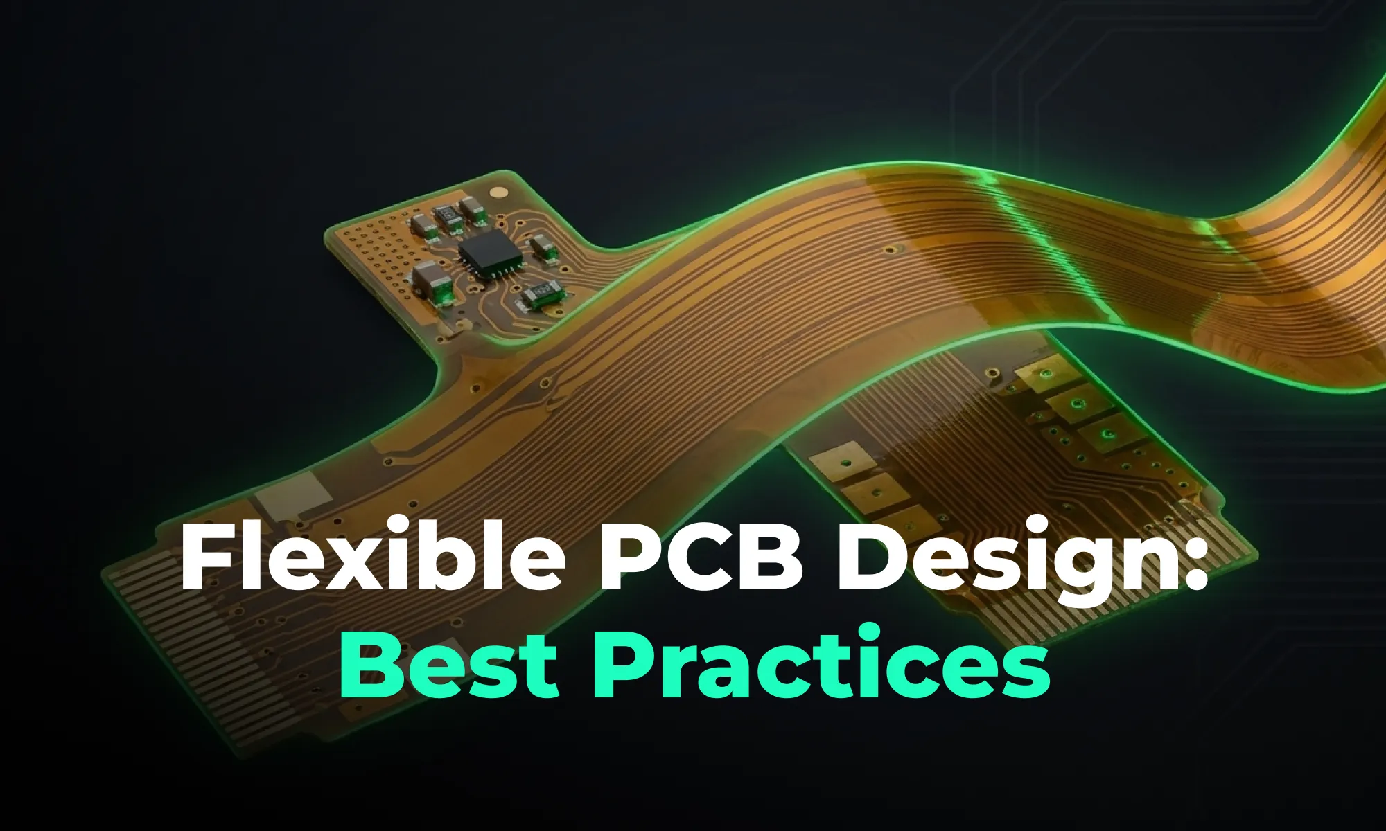
A guide to flexible PCB design, covering materials, stackups, bend radius, and layout best practices for wearables, medical devices, and other compact electronics.

A beginner-friendly guide to reading PCB schematics, covering common symbols, nets, and how to follow signal flow through a circuit diagram.

Learn the key differences between analog and digital PCB design and how to manage mixed-signal layouts for better signal integrity.

Learn how to place and select decoupling capacitors to improve power integrity in PCB design.

Learn the core rules of differential pair routing including parallel routing, consistent spacing, length matching, and return path management for high-speed PCB designs.

Learn the most common causes of PCB EMI issues and proven layout, grounding, shielding, and filtering techniques to pass EMC compliance.

Learn the most common PCB testing methods including flying probe and in-circuit testing to ensure reliability.
