

March 26, 2026
Why Dr. Juergen Kienhoefer switched to Flux after 15 years of Eagle

Share


"Once I decided to just go and move on from Eagle to Flux… I'm never going back."– Dr. Juergen Kienhoefer, RF Engineer
Dr. Juergen Kienhoefer is an experienced RF engineer based in Santa Cruz, CA, and owner of AIRcable LLC, a company focused on addressing customers’ Bluetooth range challenges. He designs custom wireless hardware for clients. His projects range from serial-to-wireless converters and RS485 controllers for modern appliances to long-range Bluetooth radios, impact sensors with directional antennas for sports, and BLE trackers. In a typical year, that work translates into about five PCB projects, often with substantial RF constraints.
What makes these builds hard is not just the circuit itself. It is the combination of RF physics, mechanical packaging, and manufacturing realities. For Juergen, the PCB design phase is a focused burst within a larger firmware-heavy project. That means the design tool has to get out of the way.
Juergen used Autodesk EAGLE for 15 years. He even held a professional license. Like many experienced engineers, familiarity was a major reason to stick with it.
But the single biggest bottleneck in his workflow was not routing or schematic capture. It was part creation, an error-prone, repetitive loop:
A single typo could derail a project and push timelines out. And it happened more than once.
"I was definitely desperate in finding something beyond EAGLE."
Juergen tried several alternatives over the years — from open-source tools to high-end commercial packages. But none of them stuck.
KiCad was the closest contender. Juergen even used it for a stretch with a former partner. But the UI proved to be a dealbreaker: after stepping away from a project for a few weeks, coming back felt like starting over. "Which mouse click, what combination? I never got it right," he said.
Commercial tools like OrCAD and Altium presented a different problem: most of them required Windows, and Juergen is not a Windows user.
So he kept searching.
Juergen came across Flux, and several things clicked quickly.

The tutorials were the gateway. Juergen described watching YouTube videos multiple times until the environment "just felt natural." That combination of guided learning plus a cloud-native tool he could access from any platform lowered the barrier enough to commit.
The ecosystem sealed the deal. Unlike EAGLE, where every part had to be built from scratch, Flux let Juergen search for components, find community-published examples, and fork working designs. Instead of spending hours on footprint and symbol creation, he could spend that time on what actually matters, schematic intent and routing.
Support kept him moving. When something broke, downtime was measured in hours instead of days. Juergen described a workflow that would be unthinkable with most EDA vendors:
"I could say, like, okay. Here's my bug report and I just go sleep and next morning it's all fixed."
He contrasted this directly with commercial tools: "Try getting someone to actually look at your board and say, what's wrong with that? No way."
AI-assisted checks added a layer of confidence. Juergen still does final verification with external Gerber viewers before sending files to manufacturing — but Flux's AI caught real mistakes he didn't realize he was making, reducing the number of issues that reach that late stage.
"The AI did help a few times finding mistakes I didn't realize making. That makes this kind of tool outstanding."
One of Juergen's standout projects in Flux is a 2.4 GHz directional patch antenna board — his most challenging build to date.
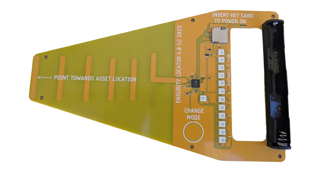
This is the type of design where small details matter:
The antenna went through three iterations — from a ceramic antenna to a piggyback sandwich design to the final integrated patch. The process spanned months of on-and-off work, but the result speaks for itself:
"I really tested the antenna… it does 10 dB — a 10 times improvement for directionality."
Juergen estimates Flux has increased his productivity by 2–4× compared to his previous EAGLE workflow. That is not "a bit faster" — it is a fundamentally different development cadence.

"Productivity increased 2–4 times than before and I expect even more in the future. We are exploring the benefits of AI integration for designing new boards. It seems very promising."
For a "known" design, a full board can be completed in roughly two weeks maximum, and not even working eight hours a day. For experimental RF work like the patch antenna, iteration spans months across multiple spins. Either way, the core benefit is the same: less time fighting setup and library work, more time making the design better.
"Flux does not have an upper limit. It gets better every time, makes it easier with every version and not just more precise but also with checks and verifications."
The shift is permanent. Every new board that he creates is now designed in Flux.


Gerber files are the universal 2D vector format that bridges PCB design and fabrication. This guide covers what each layer file contains, how to export and verify a complete manufacturing package, and the common mistakes that cause production delays.


A pi filter is a three-element passive CLC network that provides stronger ripple and EMI suppression than a single capacitor. This guide covers topology selection, component derating, resonance damping, and PCB layout best practices.

Tantalum capacitors offer high capacitance density in a tiny footprint but demand strict polarity and voltage derating. This guide explains how they compare to ceramics and aluminum electrolytics, common failure risks, and how to select and place them safely.

PCBA turns a bare PCB into a functional circuit by mounting and soldering components. This guide breaks down the assembly workflow, SMT vs through-hole methods, required manufacturing files, and common defects to avoid.

ERC checks schematic-level electrical issues while DRC checks PCB layout rules -- engineers run ERC before layout and DRC during or after routing.

The complete hardware design workflow covers requirements, schematic capture, PCB layout, validation, prototyping, and manufacturing.

PCB constraint management defines routing, spacing, impedance, and manufacturing rules and validates them throughout PCB layout.

PCB revision management tracks what changed, who changed it, and why -- keeping schematics, layout, BOM, and manufacturing files aligned.


