As modern electronics become smaller, faster, and more complex, printed circuit boards must evolve to keep pace. Gone are the days when a simple two-layer board could handle the routing and power requirements of an advanced microcontroller or high-speed data bus. Today, mastering multilayer PCB design is a fundamental requirement for hardware engineers.
Moving from single or double-sided boards to multilayer designs introduces a new world of routing capabilities, but it also brings strict rules regarding signal integrity, power distribution, and layer stackup management.
Key Takeaways
- Multilayer PCB design involves creating printed circuit boards with three or more copper layers, providing the routing space, EMI shielding, and component density needed for complex applications like IoT and robotics.
- Carefully planning the layout of signal, ground, and power planes is critical for maintaining controlled impedance and providing uninterrupted signal return paths.
- Applying proven PCB routing tips, such as routing adjacent signal layers perpendicularly and avoiding split planes, drastically reduces crosstalk and noise.
- Cloud-native, AI-assisted platforms like Flux streamline multilayer PCB layout by enabling real-time team collaboration, automated design rule checks, and intelligent routing assistance.
What Is Multilayer PCB Design?
Multilayer PCB design is the design of boards with three or more copper layers separated by dielectric materials and laminated under heat and pressure, enabling internal routing of power and high-speed signals that single- and double-layer boards cannot provide for modern digital electronics.
In modern hardware, common layer counts include:
- 4-layer boards: The standard starting point for boards featuring medium-density microcontrollers, typically structured as Signal / Ground / Power / Signal.
- 6-layer boards: Used when more routing space is needed, or when separating high-speed digital signals from sensitive analog traces.
- 8+ layer designs: Reserved for highly complex multilayer circuit board design, such as motherboards, advanced IoT gateways, or designs featuring high-pin-count Ball Grid Arrays (BGAs).
Why Multilayer PCBs Are Used in Modern Electronics?
The shift toward multilayer boards is driven by the physical constraints of modern components and the laws of physics at high frequencies. The primary benefits include:
- Higher Component Density: High-density interconnect (HDI) packages and fine-pitch BGAs simply do not have enough physical space to route all escaping traces on a single surface layer. Internal layers provide the necessary real estate.
- Improved PCB Signal Integrity: High-speed signals require a controlled impedance environment to prevent data-corrupting reflections. Internal routing adjacent to solid planes ensures predictable impedance.
- Reduced Electromagnetic Interference (EMI): By burying noisy digital traces between solid copper ground or power planes, the planes act as a Faraday cage, absorbing stray radiation and preventing external noise from coupling into the board.
- Better Power Distribution: Dedicated internal power and ground planes provide incredibly low-impedance paths for current, ensuring stable voltage delivery to power-hungry ICs while managing thermal dissipation.
Because of these advantages, multilayer architectures are mandatory for applications like IoT devices, robotics, and embedded systems.
How PCB Layer Stackup Affects Board Performance
The foundation of any high-performance board is its PCB layer stackup (the order and spacing of conductive copper and insulating dielectric layers in a PCB). Stackup planning involves determining the order of signal layers, ground planes, and power planes, as well as the thickness and dielectric constant of the materials between them.
Proper multilayer PCB stackup design dictates how electromagnetic fields propagate through your board.
Common Multilayer Stackup Configurations
| Layer Count |
Typical Arrangement |
Best Used For |
Key Advantages |
| 4-Layer |
Top Signal, Ground Plane, Power Plane, Bottom Signal |
Standard microcontrollers, simple IoT sensors, and basic industrial controls. |
Cost-effective step up from 2-layer boards; provides basic EMI shielding and a solid return path for signals. |
| 6-Layer |
Signal, Ground Plane, Inner Signal, Power Plane, Ground Plane, Signal |
Devices requiring dedicated high-speed routing, mixed-signal designs, and dense component placements. |
Safely buries sensitive high-speed traces internally; provides excellent impedance control and better EMI reduction. |
| 8-Layer |
Signal, Ground, Signal, Ground/Power, Ground/Power, Signal, Ground, Signal |
Advanced motherboards, FPGA designs, high-pin-count BGAs, and RF applications. |
Maximum routing flexibility; isolates multiple power domains; superior electromagnetic compatibility (EMC) and thermal dissipation. |
Key Stackup Considerations:
- Signal Return Paths: High-frequency current typically follows the path of least inductance, which usually means directly beneath the signal trace on the nearest reference plane. A good PCB ground plane design ensures an uninterrupted return path.
- Impedance Control: The distance between a signal layer and its reference plane dictates trace impedance (e.g., 50Ω single-ended).
- EMI Reduction: Keep high-speed signal layers tightly coupled (physically close) to their respective ground planes to contain electromagnetic fields.
Best Multilayer PCB Routing Practices
Once your stackup is defined, the routing phase (process of connecting components with copper traces according to the schematic) begins. Executing a clean layout requires strict adherence to PCB routing best practices to avoid cross-coupling and timing errors.
- Alternate Routing Directions: If you have adjacent signal layers (e.g., layers 3 and 4), route traces on one layer horizontally (X-axis) and the other vertically (Y-axis). This minimizes broadside coupling (crosstalk) between the layers.
- Keep Traces Short: Especially for high-speed digital clocks and analog inputs. Shorter traces have less parasitic inductance and capacitance.
- Separate Analog and Digital Signals: Never route noisy digital traces through an analog section of the board, and do not allow them to share the same return path space on the ground plane.
- Differential Pair Routing: Route high-speed differential pairs (like USB or HDMI) perfectly parallel, matched in length, and completely symmetrical to ensure common-mode noise rejection (the ability to suppress noise appearing equally on both signal lines)..
Multilayer Routing Best Practices Checklist
- Route adjacent signal layers in perpendicular directions.
- Use dedicated, solid ground planes (avoid splitting them unless strictly necessary).
- Keep high-speed signals short and route them on layers adjacent to a ground plane.
- Minimize unnecessary vias, as each via introduces an impedance discontinuity.
- Place decoupling capacitors on the top/bottom layers as close to the IC power pins as possible, dropping immediately to the internal power/ground planes.
Common Multilayer PCB Design Mistakes
Even experienced engineers can run into issues during complex layouts. Avoid these common pitfalls:
-
⚠ Error
Poor Layer Stackup Planning
Routing high-speed signals on an inner layer that is sandwiched between two other signal layers (instead of planes) guarantees severe crosstalk and EMI issues.
-
⚠ Error
Improper Ground Plane Placement
Creating a "split plane" (routing a void through the copper) and then routing a high-speed trace directly over that split. This destroys the return path, creating a massive loop antenna that radiates noise.
-
⚠ Error
Excessive Vias (The Swiss Cheese Effect)
Placing too many vias too close together can create excessive holes in your internal ground plane that it effectively creates a continuous void, obstructing return currents.
-
⚠ Error
Signal Crosstalk from Poor Trace Spacing
Failing to maintain the "3W Rule" (keeping the distance between trace centers at least three times the trace width) for high-speed nets.
How Modern PCB Tools Simplify Multilayer Design
Historically, multilayer PCB layout was performed on rigid, desktop-based EDA software that kept engineers siloed and required tedious manual constraint programming. Today, cloud-native, modern platforms like Flux are fundamentally shifting how hardware teams collaborate.
By bringing PCB design into the browser, modern tools offer a "multiplayer" environment where electrical engineers, layout designers, and mechanical engineers can view and edit the same board simultaneously.
Flux: Collaborative, Browser-Based Electronics Design
Flux is a modern EDA platform built for the way hardware teams actually work today, in the browser, collaboratively, and with tight schematic-to-PCB integration.
-
Real-time collaboration
Multiple engineers can work on the same schematic at the same time, the same way you'd collaborate in a Google Doc. No more locked files or waiting your turn.
-
Browser-based access
No installs, no license servers, no OS headaches. Open your design from any device and pick up where you left off.
-
Unified schematic and PCB environment
The handoff from schematic to PCB layout happens inside the same platform, so nothing gets lost in translation between tools.
-
Automated design validation
Built-in ERC catches connectivity issues, missing power references, and symbol errors in real time before they propagate into layout.
-
Version control and design history
Every change is tracked, making it easy to review diffs, roll back to earlier revisions, and understand why a design decision was made.
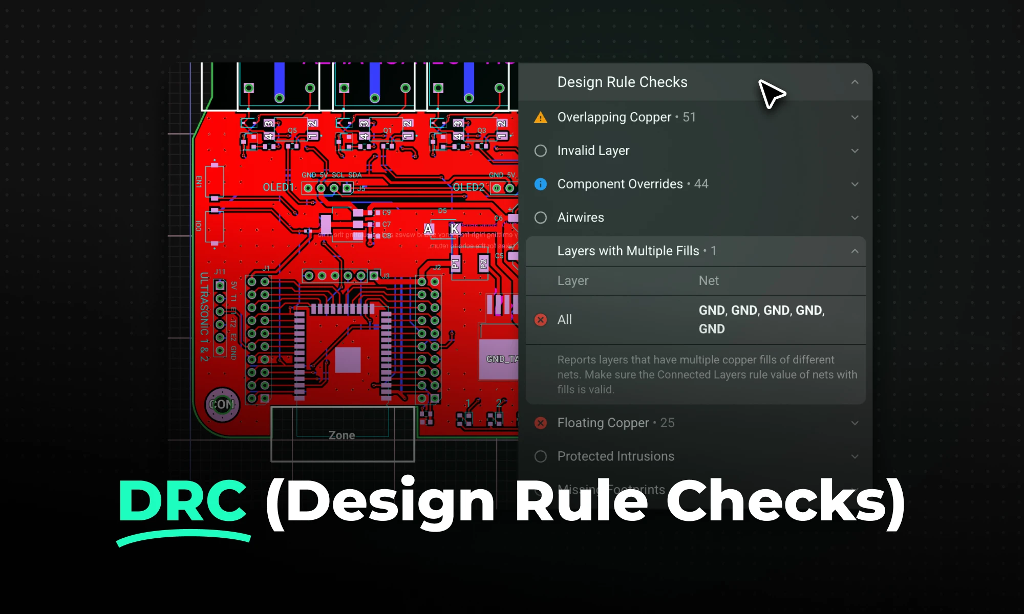
Platforms like Flux also integrate AI directly into the workflow. Instead of manually cross-referencing datasheets for an 8-layer stackup or struggling to untangle a BGA breakout, hardware teams can leverage AI-assisted routing suggestions and an AI Copilot to check for PCB signal integrity risks, automate part selection, and run real-time design rule checks (DRCs). This drastically reduces the mental overhead of multilayer design, allowing engineers to iterate faster and catch errors before fabrication.
FAQs
What is multilayer PCB design? ▾
Multilayer PCB design is the engineering process of creating a printed circuit board with three or more conductive copper layers. These layers are separated by dielectric material and allow for higher component density and complex internal routing.
How many layers should a PCB have? ▾
The required number of layers depends entirely on circuit complexity and component density. Simple sensor nodes might only need 4 layers, while modern smartphones and computer motherboards often require 10, 12, or 16+ layers to route all signals and provide adequate ground shielding.
Why are ground planes important in multilayer PCBs? ▾
Ground planes provide a low-impedance return path for electrical currents, which is vital for maintaining signal integrity. They also act as electromagnetic shields, preventing noise from coupling between adjacent signal layers or radiating off the board.
What are common multilayer PCB routing challenges? ▾
Common challenges include managing impedance control across different layers, safely breaking out traces from high-density BGA packages, minimizing crosstalk between adjacent traces, and avoiding vias that disrupt internal ground planes.
What software is used to design multilayer PCBs? ▾
Engineers use Electronic Design Automation (EDA) software to design multilayer PCBs. While legacy desktop tools have been the standard for decades, modern teams are increasingly moving to browser-based, AI-assisted, collaborative platforms like Flux to accelerate their design cycles.