April 21, 2026
PCB Prototyping vs. Fabrication: Which Process Is Right for Your Project?
Share

In hardware development, rushed circuit design, inadequate validation, and skipping prototype iterations are common pitfalls that lead to wasted time, money, and materials. Creating electronics is a process that requires validation through each stage. Two of the most critical stages in this process are prototyping and fabrication.
While these terms are sometimes used interchangeably by beginners, they represent entirely different mindsets, goals, and manufacturing processes. Understanding the difference between a PCB prototype and a full-scale production run is essential for any hardware engineer, startup founder, or product developer looking to bring a device to market successfully. This guide breaks down the definitions, trade-offs, and decision points to help you choose the right path for your project.
PCB prototyping is the practice of manufacturing a small number of circuit boards (usually between 1 and 10) to test a new or unverified design. The primary goal of a PCB prototype is validation. Engineers use prototypes to prove that their schematic logic works in the real world, to test the physical fit of the board within an enclosure, and to debug any signal integrity or power issues.
Because the focus is on testing and rapid iteration rather than perfection or unit cost, prototypes are often manufactured using looser tolerances, cheaper materials, or standardized "pool" panels at the fab house to speed up delivery times. It is completely normal and expected for a prototype board to require manual modifications, such as cutting traces with a knife or soldering "jumper wires" to fix mistakes.
A prototype should be designed as a testing tool, not just a pre-production board. The goal is to make validation, debugging, and iteration as easy as possible.
Include clearly labeled test points for key signals like power rails, communication lines, and clocks so they can be measured quickly. Add jumper pads or zero-ohm resistor footprints to allow signal rerouting, isolation, or quick fixes without a redesign. Ensure there is enough space for probes so tools can access critical nodes without difficulty.
In the context of this comparison, PCB fabrication refers to the full-scale, production-ready manufacturing of a finalized circuit board design.
Once a design has been rigorously tested through multiple prototype iterations and bugs have been resolved, it is ready for fabrication. The goals here shift dramatically: the focus is no longer on testing, but on scalability, cost-per-unit reduction, and uncompromising quality and consistency.
Production fabrication involves setting up dedicated manufacturing lines, creating custom solder stencils, and running automated optical inspection (AOI) and electrical testing on every single board. The boards produced in this stage are the ones that will ultimately end up in the hands of the consumer.
Understanding PCB prototyping vs fabrication requires looking at the practical trade-offs between the two processes. Manufacturers optimize their equipment differently depending on which service you request.
| Feature | PCB Prototyping | Production Fabrication |
|---|---|---|
| Primary Goal | Testing, debugging, and proof-of-concept. | Scalability, reliability, and end-user deployment. |
| Volume | Low (Typically 1 to 20 boards). | High (Hundreds to millions of boards). |
| Speed (Turnaround Time) | Fast (Often 24 hours to 5 days). | Slower setup (Typically 2 to 4 weeks or more). |
| Cost Per Board | High (Due to setup costs spread over few units). | Low (Economies of scale drastically reduce unit price). |
| Design Changes | Expected and frequent. | Highly discouraged; requires expensive re-tooling (ECOs). |
| Testing & Quality Control | Basic electrical testing; visual inspection. | Rigorous automated testing (AOI, X-Ray, flying probe) on every unit. |
| Materials & Tolerances | Often uses standard materials (FR4) and relaxed tolerances for speed. | Uses specific, requested materials and strict adherence to IPC Class 2 or 3 standards. |
Deciding which PCB manufacturing method to use depends entirely on where you are in the product development lifecycle.
When to Use PCB Prototyping:
When to Use PCB Fabrication (Production):
The prototype to production process is rarely a straight line. Many hardware teams fall into common traps that derail their timelines and budgets:
The transition from prototype to production is where the concept of Design for Manufacturability (DFM) becomes critical.
During the prototyping phase, a designer might ignore a minor DFM warning (like placing a component slightly too close to the board edge) because a technician can manually assemble a few boards with care. However, if that same design is pushed to automated production fabrication, that minor error will cause pick-and-place machines to crash or boards to crack during depanelization, ruining the entire batch.
Validating your design using design rule checks (DRC), panelization reviews, and assembly clearances against strict production manufacturing rules during the final prototype stage is essential for a smooth transition. This can be done by running fabrication and assembly rule checks in your ECAD tool, reviewing panel layouts with your manufacturer, and confirming component spacing, fiducials, and tooling holes meet automated assembly requirements.
The traditional PCB development process often involves isolated engineers working on desktop software, emailing design files back and forth, and waiting weeks for prototype boards to arrive, only to find an easily preventable error.
Modern, cloud-native platforms like Flux are fundamentally changing how teams approach PCB iteration design. Flux provides a collaborative environment where electrical engineers, firmware developers, and mechanical designers can review the same schematic and layout simultaneously in real-time.
By utilizing built-in, real-time design rule checks, Flux helps teams catch errors before the first prototype is ever ordered. This immediate feedback loop drastically accelerates design iteration cycles, reducing the number of physical prototypes required to achieve a working board. When the design is finally verified, Flux generates the manufacturing files needed to transition confidently from a rapid prototype to full-scale fabrication.
Now that you understand the distinction between PCB prototyping and fabrication, it's time to put that knowledge into practice. Whether you're validating your first schematic or preparing for a production run of thousands of boards, having the right tools makes all the difference. Flux's cloud-native platform gives you real-time design rule checking, collaborative review, and seamless manufacturing file generation, all in your browser. Ready to accelerate your hardware development workflow? Sign up for Flux today and start building with confidence.


How hardware teams apply Git-style version control to PCB design — tracking revisions, collaborating safely, and maintaining a complete design history.

A checklist for PCB design documentation -- covering the files, drawings, and release data every manufacturing package should include.

A practical guide to PCB library management -- how hardware teams standardize components, centralize libraries, and scale collaborative design workflows.
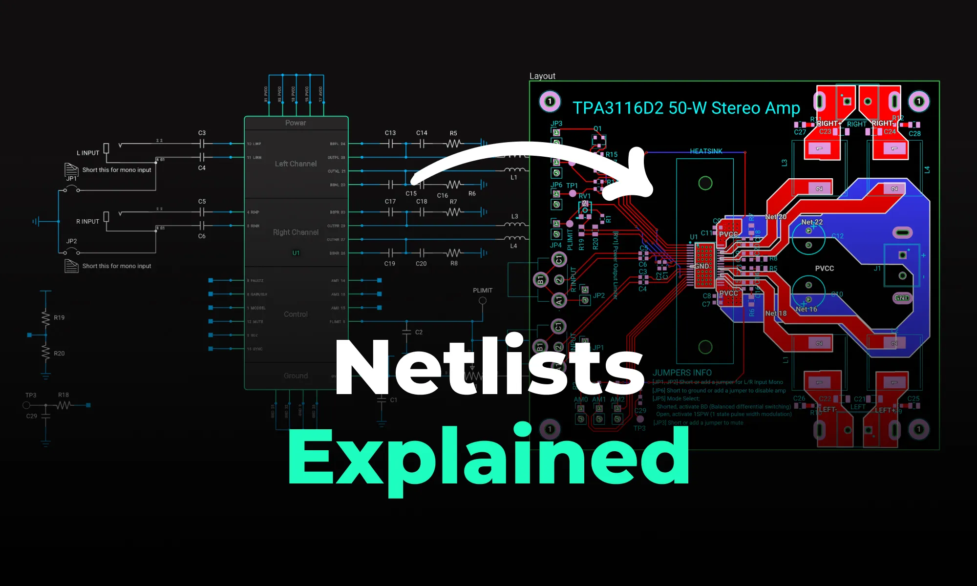
An engineer-friendly explainer of PCB netlists -- what they contain, how they are generated, and how they connect schematic capture to PCB layout.
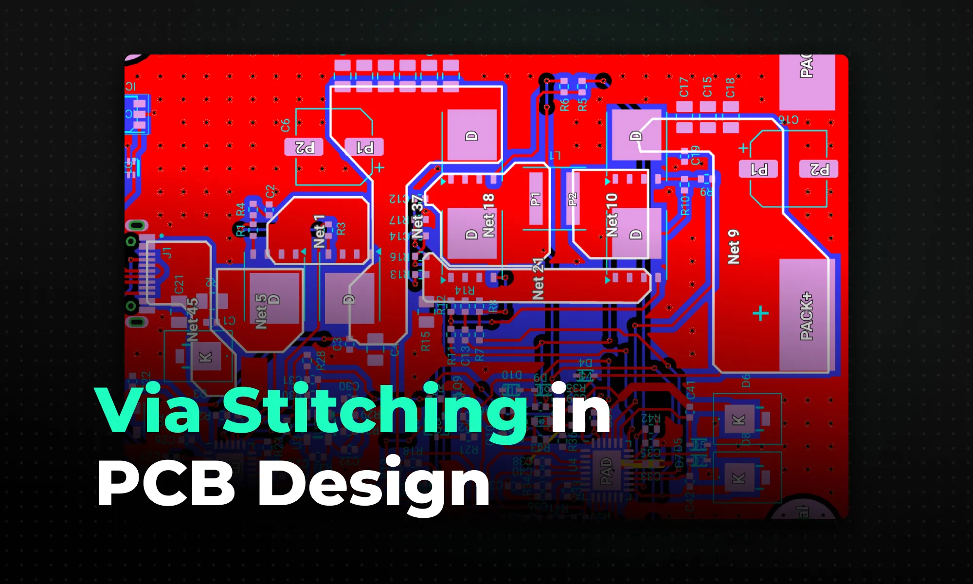
A practical guide to via stitching in PCB design -- what it is, why it improves EMI, signal integrity, and thermal performance, and where to place stitching vias. Includes spacing rules (like lambda/20), design guidelines, common mistakes to avoid, and how Flux can automate stitching via placement.

A guide to PCB component selection, covering electrical specs, footprints, thermal performance, sourcing, and best practices for picking parts that ship reliably.

A guide to PCB design reviews, covering schematic, layout, and DFM checks engineers use to catch errors early and ship more reliable boards.

A guide to creating and managing PCB footprint libraries, covering IPC standards, pad sizing, validation workflows, and best practices for reliable land patterns.
