Oscillators
An oscillator is an electronic circuit that generates a periodic, oscillating signal, often a sine wave or a square wave. Oscillators are used in a wide range of applications, including clocks, radios, and sound synthesis. Flux.ai has the world's largest community-driven public library of oscillators, with footprints, symbols, datasheets, and simulation models. This comprehensive resource allows engineers and designers to easily find the oscillator they need for their specific application and use it with confidence. Whether you are working on a simple clock circuit or a complex radio transmitter, Flux.ai's oscillator library has you covered. So, if you are in need of an oscillator for your next project, be sure to check out Flux.ai's extensive collection.
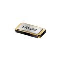
XTL721-S999-301
32.768 kHz ±20ppm Crystal 9pF 70 kOhms 2-SMD, No Lead The XTL721-S999-301 specification defines the engineering requirements for a crystal oscillator component intended to provide a stable and accurate timing reference for electronic systems. This specification establishes the functional, electrical, mechanical, environmental, and quality requirements necessary to ensure precise frequency generation, reliable operation, and long-term stability in embedded, industrial, communication, and consumer electronic applications. The component is intended for use in applications requiring accurate clock generation and synchronization, including microcontroller-based systems, communication interfaces, digital signal processing, and timing circuits. It provides a highly stable frequency reference with low phase noise and excellent frequency stability to support reliable system operation under varying environmental conditions. Engineering Requirements The crystal component shall be manufactured using high-purity quartz material and precision fabrication processes to ensure consistent resonant frequency characteristics, low aging effects, and dependable long-term performance. The construction shall provide stable oscillation characteristics throughout the specified operating temperature and environmental conditions. Electrical characteristics shall ensure accurate frequency stability, low equivalent series resistance, and reliable oscillation startup when used with compatible oscillator circuits. The component shall maintain stable timing performance under normal supply variations, temperature fluctuations, and continuous operating conditions. Mechanical construction shall be suitable for automated surface-mount assembly and compatible with standard solder reflow manufacturing processes. The package shall provide mechanical robustness and resistance to vibration, mechanical shock, thermal cycling, and handling without degradation of electrical performance or structural integrity. Workmanship shall be free from defects including contamination, package cracking, seal failure, lead deformation, or structural inconsistencies that could adversely affect frequency accuracy or operational reliability. Inspection, validation, and testing shall be performed using calibrated equipment and controlled quality procedures to verify compliance with engineering and manufacturing requirements. Any deviation from this specification shall require formal engineering evaluation, documented technical justification, and approval through the established engineering change control process before implementation. Documentation Supporting documentation shall include engineering drawings, frequency performance specifications, electrical characterization reports, qualification records, inspection reports, reliability data, material declarations, and revision-controlled manufacturing documentation. All documentation shall be maintained under formal configuration management and quality assurance systems to ensure complete product traceability. Revision Control Any modification to this specification shall be managed through the formal engineering change management process. All revisions shall undergo technical review, validation, and approval before release to ensure continued compliance with design intent and applicable engineering standards. #EngineeringSpecification #CrystalOscillator #QuartzCrystal #TimingDevice #ClockGenerator #EmbeddedSystems #IndustrialElectronics #FrequencyControl #QualityAssurance #EngineeringDocumentation
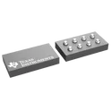
0 Uses0 StarsMSPM0C1104S8YCJR
ARM® Cortex®-M0+ MSPM0 C Microcontroller IC 32-Bit 24MHz 16KB (16K x 8) FLASH 8-DSBGA (0.86x1.6) MSPM0C110x microcontrollers (MCUs) are part of the MSP highly-integrated ultra-low-power 32-bit MCU family based on the enhanced Arm® Cortex®-M0+ core platform operating at up to 24MHz frequency. These costoptimized MCUs offer high-performance analog peripheral integration, support extended temperature ranges from -40°C to 125°C, and operate with supply voltages from 1.62V to 3.6V. The MSPM0C110x devices provide up to 16KB embedded flash program memory with 1KB SRAM. These MCUs incorporate a high-speed on-chip oscillator with an accuracy from -2% to +1.2%, eliminating the need for an external crystal. Additional features include a 1-channel DMA, CRC-16 accelerator, and a variety of highperformance analog peripherals such as one 12-bit 1.5Msps ADC with VDD as the voltage reference, and an on-chip temperature sensor. These devices also offer intelligent digital peripherals such as one 16-bit advanced timer, two 16-bit general purpose timer, one windowed watchdog timer, and a variety of communication peripherals including one UART, one SPI, and one I2C. These communication peripherals offer protocol support for LIN, IrDA, DALI, Manchester, smart card, SMBus, and PMBus. The TI MSPM0 family of low-power MCUs consists of devices with varying degrees of analog and digital integration let customers find the MCU that meets their project needs. The architecture combined with extensive low-power modes is optimized to achieve extended battery life in portable measurement applications. MSPM0C110x MCUs are supported by an extensive hardware and software ecosystem with reference designs and code examples to get the design started quickly. Development kits include a LaunchPad™ kit available for purchase and design files for a target-socket board. TI also provides a free MSP Software Development Kit (SDK), which is available as a component of Code Composer Studio™ IDE desktop and cloud version within the TI Resource Explorer. MSPM0 MCUs are also supported by extensive online collateral, training with MSP Academy, and online support through the TI E2E™ support forums. Features • Core – Arm® 32-bit Cortex®-M0+ CPU, frequency up to 24MHz • Operating characteristics – Extended temperature: –40°C to 125°C – Wide supply voltage range: 1.62V to 3.6V • Memories – Up to 16KB of flash – 1KB of SRAM • High-performance analog peripherals – One analog-to-digital converter (ADC) with up to 10 total external channels, 1.7Msps at 10 bit or 1.5Msps at 12 bit with VDD as the voltage reference – Configurable 1.4V or 2.5V internal ADC voltage reference (VREF) – Integrated temperature sensor – Integrated supply monitor • Optimized low-power modes – RUN: 87µA/MHz – STOP: 609µA at 4MHz, 311µA at 32kHz – STANDBY: 5µA with SRAM retention – SHUTDOWN: 200nA • Intelligent digital peripherals – 1-channel DMA controller dedicated for ADC – Three timers supporting up to 14 PWM channels • One 16-bit advanced timers with deadband support up to 8 PWM channels • One 16-bit general purpose timer with 4 capture/compares • One 16-bit general purpose timer with 2 capture/compares – Windowed watchdog timer – BEEPER generating 1kHz, 2kHz, 4kHz, or 8kHz square wave to drive the external beeper • Enhanced communication interfaces – One UART interface supporting LIN, IrDA, DALI, smart card, Manchester and low-power operation in STANDBY mode – One I2C interface supporting FM+ (1Mbps), SMBus, PMBus, and wakeup from STOP mode – One SPI supporting up to 12Mbps • Clock system – Internal 24MHz oscillator with an accuracy from -2% to +1.2% (SYSOSC) – Internal 32kHz low-frequency oscillator (LFOSC) • Data integrity – Cyclic redundancy checker (CRC-16) • Flexible I/O features – Up to 18 GPIOs – Two 5V-tolerant open-drain IOs • Development support – 2-pin serial wire debug (SWD) • Package options – 20-pin TSSOP (PW) – 20-pin VSSOP (DGS) – 20-pin WQFN (RUK) – 16-pin SOT (DYY) – 8-pin SOT (DDF) – 8-pin WSON (DSG) – 8-pin DSBGA (YCJ) • Family members (also see Device Comparison) – MSPS003F4: 16KB of flash, 1KB of RAM – MSPS003F3: 8KB of flash, 1KB of RAM – MSPM0C1104: 16KB of flash, 1KB of RAM – MSPM0C1103: 8KB of flash, 1KB of RAM • Development kits and software (also see Tools and Software) – LP-MSPM0C1104 LaunchPad™ development kit – MSP Software Development Kit (SDK) 2 Applications • Battery charging and management • Power supplies and power delivery • Personal electronics • Building security and fire safety • Connected peripherals and printers • Grid infrastructure • Smart metering • Communication modules • Medical and healthcare • Lighting #MSPM0C1104S8YCJR #MSPM0C1104 #TexasInstruments #CortexM0Plus #Microcontroller #EmbeddedSystems #LowPowerMCU #IoT #WearableDevices #IndustrialControl #ConsumerElectronics #ADC #UART #SPI #I2C #PWM #TI #ElectronicsDesign #PCBDesign #EmbeddedDevelopment
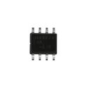
2 Uses0 StarsXL1509-5.0E1
2A 150KHz 40V Buck DC to DC Converter The XL1509-5.0E1 is a fixed frequency PWM buck step-down DC-DC converter capable of driving a load with high efficiency, low ripple, and excellent line and load regulation. It is manufactured by XLSEMI and belongs to the XL1509 product family, a series of fixed-output and adjustable-output step-down switching regulator ICs designed to simplify the design of compact, efficient DC power conversion stages in a wide range of embedded, industrial, and consumer electronics applications. The "5.0" designation in the part number specifies that this variant produces a fixed regulated output voltage of five volts, making it directly suited to powering five-volt logic, microcontrollers, sensors, communication modules, and other standard digital subsystems from higher-voltage DC rails without requiring a linear regulator and its inherent power dissipation penalty. Unikeyic Electronics The XL1509 requires a minimum number of external components, making it simple to use, and includes internal frequency compensation and a fixed-frequency oscillator. The PWM control circuit is able to adjust the duty ratio linearly from zero to one hundred percent. This internal compensation architecture removes the burden of control loop design from the system engineer, which is a common point of complexity in discrete buck converter designs, and allows the device to be implemented with a straightforward application circuit consisting of an input capacitor, an output inductor, a freewheeling Schottky diode, and an output capacitor, without requiring additional feedback network components in the fixed-output version. Unikeyic Electronics The device operates across a wide input voltage range, accepting input rails ranging from just above the output voltage all the way up to the high end of the input range, making it compatible with a variety of common source voltages including twelve-volt, twenty-four-volt, and other industrial bus rails frequently encountered in embedded and industrial power system designs. This wide input range also makes it suitable for battery-powered applications where the supply voltage varies considerably across the battery discharge cycle, as the converter maintains a regulated output throughout the input voltage window. The fixed switching frequency is set internally at a value that represents a practical tradeoff between external component size and switching loss, allowing the use of standard commodity inductors and electrolytic or ceramic output capacitors without requiring unusually large or small values. An enable function and an overcurrent protection function are built inside. When a secondary current limit condition occurs, the operating frequency is reduced to a lower switching frequency, which limits the energy delivered per cycle and prevents damage to the power switch and external components during sustained overload events. This dual-level current protection approach provides both instantaneous peak current limiting and sustained overload protection, improving the robustness of designs built around the device in applications where load transients or fault conditions may cause temporary overcurrent conditions. Unikeyic Electronics The device is housed in a standard eight-pin small-outline integrated circuit surface-mount package, making it compatible with automated pick-and-place and reflow soldering assembly processes and suitable for compact power supply layouts on densely populated PCBs. Spec Sheet Identification Part Number: XL1509-5.0E1 Device Family: XL1509 Buck DC-DC Converter Series Manufacturer: XLSEMI Part Number Decode XL1509: Base device family 5.0: Fixed output voltage — five volts E1: Tape-and-reel packaging variant Functional Classification Device Type: Fixed-frequency PWM step-down buck DC-DC converter IC Topology: Non-synchronous buck converter with internal power switch Output Configuration: Single output, fixed voltage Regulation Method: Fixed-frequency PWM with internal compensation Electrical Characteristics Input Voltage Range: Wide input range, compatible with common industrial and consumer DC bus voltages Output Voltage: Fixed regulated output at five volts Output Current: Continuous rated current class suitable for moderate embedded system loads Switching Frequency: Fixed internal oscillator, mid-frequency class Duty Cycle Range: Adjustable from zero to maximum, internally controlled Minimum Dropout Voltage: Low dropout class Output Ripple: Low ripple characteristic with appropriate external filter components Control & Protection Features Enable Function: Built-in enable control input for power sequencing and shutdown Overcurrent Protection: Integrated primary current limit with frequency fold-back secondary protection Internal Compensation: Built-in frequency compensation, no external compensation network required Feedback: Internal reference for fixed output voltage regulation External Components Required Input Capacitor: Required for input decoupling Output Inductor: Required, standard commodity value Freewheeling Diode: External Schottky diode required Output Capacitor: Required for output filtering Environmental & Qualification Operating Temperature Range: Industrial range, below zero to elevated ambient RoHS Compliance: Yes, Halogen-Free Package Package Type: SOIC-8 (SOP-8) Mounting Method: Surface mount technology (SMT) Packaging Format Supply Format: Tape-and-reel Reel Quantity: Standard production reel quantity Available Variants in XL1509 Family XL1509-3.3E1: Fixed output at regulated lower voltage XL1509-5.0E1: Fixed output at five volts (this device) XL1509-12E1: Fixed output at twelve volts XL1509-ADJE1: Adjustable output version #XL1509 #XL15095 #XLSEMI #BuckConverter #StepDownConverter #DCDCConverter #PWMConverter #SwitchingRegulator #PowerManagement #EmbeddedPower #FixedOutputConverter #FiveVoltRegulator #IndustrialPower #SOIC8 #SurfaceMount #LowRipple #HighEfficiency #SemiconductorIC #EngineeringSpec #ComponentLibrary #CommonPartsLibrary #RoHSCompliant #PCBDesign
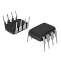
17 Uses0 StarsICM7555IPA+
Timer ICM7555IPA+ DIP-8_L10.1-W6.3-P2.54-LS7.6-BL LCSC Part Number: C1520201 ICM7555 / ICM7556 CMOS Precision Timer – low-power general-purpose timer IC compatible with the classic 555 timer architecture. Available as a single timer (ICM7555) or dual timer (ICM7556). Designed for accurate timing, pulse generation, pulse-width modulation (PWM), frequency generation, delay circuits, oscillators, and sequential timing applications. Features ultra-low supply current, wide operating voltage range (2 V to 18 V), TTL compatibility, adjustable duty cycle, and improved CMOS performance compared to standard bipolar 555 timers. Search Keywords: ICM7555, ICM7556, CMOS 555 Timer, Precision Timer IC, Low Power Timer, General Purpose Timer, PWM Generator, Pulse Generator, Oscillator IC, Delay Timer, Monostable Multivibrator, Astable Multivibrator, Frequency Generator, Timing Circuit, CMOS Timer, Analog Timer IC, Low Power Oscillator, Dual Timer IC, Single Timer IC, 555 Compatible Timer Hashtags: #ICM7555 #ICM7556 #CMOS555 #555Timer #TimerIC #PrecisionTimer #PulseGenerator #PWMGenerator #OscillatorIC #FrequencyGenerator #DelayCircuit #Monostable #Astable #CMOS #LowPowerElectronics #AnalogIC #EmbeddedSystems #ElectronicsDesign #CircuitDesign #PCBDesign
20 Uses0 StarsLORA-CC68-915MHz-TCXO
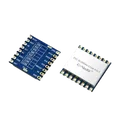
LORA-CC68-915MHz-TCXO is a compact, high-performance LoRa wireless transceiver module from NiceRF based on the Semtech LLCC68 chipset. Operating in the 915 MHz ISM band, it features a high-precision TCXO (Temperature-Compensated Crystal Oscillator) for improved frequency stability, making it ideal for long-range, low-power IoT and industrial wireless communication applications. The module supports LoRa, FSK, and GFSK modulation schemes, provides up to +22 dBm (160 mW) transmit power, and achieves receiver sensitivity as low as -129 dBm for extended communication range. It communicates through an SPI interface and is optimized for battery-powered and low-power systems. Key Features Based on Semtech LLCC68 LoRa transceiver chip 915 MHz ISM band operation High-precision TCXO for enhanced frequency stability Supports LoRa, FSK, and GFSK modulation Up to +22 dBm (160 mW) RF output power Receiver sensitivity up to -129 dBm SPI communication interface Operating voltage: 1.8 V to 3.7 V Low receive current (~6.5 mA typical) Integrated antenna switching circuitry Compact 16 mm × 16 mm SMD package Suitable for long-range and low-power wireless applications FCC-certified 915 MHz version RoHS compliant Typical Applications Smart Metering Industrial Automation Agricultural Monitoring Smart Cities Environmental Sensors Asset Tracking Warehouse Management Remote Control Systems Street Lighting Control Battery-Powered IoT Devices #CommonPartsLibrary #Module #LoRa #LLCC68 #915MHz #TCXO #WirelessModule #RFModule #IoT #IndustrialAutomation #SmartMetering #LongRangeCommunication #LowPowerDesign #SPI #EmbeddedSystems #NiceRF
0 Uses0 StarsCD4046BE
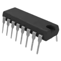
Phase Lock Loop (PLL) IC 2.4MHz 1 16-DIP (0.300", 7.62mm) CD4046BE is a CMOS Micropower Phase-Locked Loop (PLL) integrated circuit that combines a linear Voltage-Controlled Oscillator (VCO), two phase comparators, a source follower, and a Zener diode in a single package. It is designed for frequency synthesis, frequency detection, FM demodulation, clock recovery, motor speed control, and other synchronization applications. The device operates over a wide supply voltage range and offers low power consumption, high noise immunity, and excellent VCO linearity. Key Features Wide operating supply voltage range: 3 V to 18 V Integrated Voltage-Controlled Oscillator (VCO) Two selectable phase comparators for flexible PLL design Operating frequency range up to approximately 1.4 MHz Very low power consumption High VCO linearity (typically <1%) Low frequency drift with temperature VCO inhibit control for ON/OFF keying applications Built-in source follower output for demodulation applications High noise immunity characteristic of CMOS technology Available in 16-pin PDIP (CD4046BE) package Typical Applications Frequency synthesis and multiplication FM modulation and demodulation Frequency discrimination Clock recovery and data synchronization Tone decoding Voltage-to-frequency conversion FSK modulation/demodulation Motor speed control systems Signal tracking and phase synchronization circuits Hashtags #CD4046BE #PLL #PhaseLockedLoop #VCO #ClockRecovery #FrequencySynthesizer #FMDemodulator #FSKModulation #CMOS #TexasInstruments #AnalogIC #TimingIC #SignalProcessing #EmbeddedSystems #ElectronicsDesign
4 Uses0 StarsMS2130
USB 3.0 high-definition video capture chip MacroSilicon Technology Co., Ltd. MS2130 is a USB 3.0 high-definition video and audio capture IC designed to convert HDMI/DVI input signals into USB video and audio streams. It integrates a USB 3.0 device controller, data transceiver, and audio/video processing modules, allowing HD video capture and preview on PCs, smartphones, and tablets through a USB interface. The device supports UVC/UAC standards and provides YUV422 and MJPEG video output formats for broad operating system compatibility. Key Features: HDMI 1.4b receiver with DVI 1.0 compatibility Supports HDCP 1.4 Maximum HDMI input resolution up to 4K (3840 × 2160) @ 30Hz Supports RGB444, YCbCr422, YCbCr444, and YCbCr420 color formats Supports deep color modes (24/30/36-bit) Integrated USB 3.0 device controller and transceiver USB 2.0 device mode compatibility Supports USB Video Class (UVC 1.0) and USB Audio Class (UAC 1.0) Video output supports YUV422 and MJPEG formats Default USB video output up to 1920 × 1080 @ 60Hz USB audio output with 48 kHz stereo support Compatible with Windows, Android, Linux, and macOS systems Requires external 24 MHz crystal oscillator Integrated PLL and power-on reset circuitry Available in QFN-64-EP (9 mm × 9 mm) package RoHS compliant Applications: HDMI to USB capture devices Video streaming equipment Online conferencing devices Embedded video acquisition systems Portable multimedia devices Hashtags: #MS2130 #MacroSilicon #USB30 #HDMICapture #VideoCaptureIC #HDMIToUSB #USBVideo #EmbeddedSystems #VideoProcessing #UVC #UAC #QFN64 #ElectronicsDesign #PCBDesign
0 Uses0 StarsCH9329
Serial Port to HID Keyboard and Mouse Chip CH9329 is a UART to standard USB HID device (keyboard, mouse, custom HID) chip. According to different operating modes, it can be identified as the standard USB keyboard device, USB mouse device or custom HID device on the computer. CH9329 receives serial port data sent from the client and according to the HID device specification, the data will be packaged and then transmitted to the computer via USB port. Though the provided computer software, users can also configure the chip operating mode, serial communication mode, serial communication baud rate, various timeout periods, VID, PID, and various USB string descriptors. Features l Supports 12Mbps full-speed USB transmission, USB 2.0compatible, built-in crystal oscillator. l Default serial baud rate is 9600bps, which supports various common baud rates. l Supports 5V and 3.3V power voltage. l Multiple chip operating modes to adapt to different application requirements. l Flexible switching among multiple serial communication modes. l Supports normal keyboard and multimedia keyboard function, and supports full keyboard function. l Supports absolute mouse and relative mouse functions. l Supports custom HID device functions, which can be used for pure data transmission. l Supports ASCII code characters input and section-position code Chinese characters input. l Supports remote computer wake-up function. l Supports to configure VID, PID, and various USB string descriptors of chip. l Supports to configure default baud rate of chip. l Supports to configure communication address of chip to realize multiple chips hanged on the same serial port. l Supports to configure “Enter” character. l Supports to configure filter string to filter invalid characters conveniently. l Complies with USB related specifications and HID device related specifications. l RoHS compliant SOP-16 lead-free package.
4 Uses0 StarsTSX-3225_26.0000MF09Z-AC0
26 MHz ±10ppm Crystal 9pF 40 Ohms 4-SMD, No Lead # TSX-3225 26.0000MF09Z-AC0 ## General Description The TSX-3225 26.0000MF09Z-AC0 is a high-precision surface-mount quartz crystal manufactured by Seiko Epson Corporation. It is designed to provide a stable and accurate clock reference for microcontrollers, wireless communication modules, RF transceivers, processors, and other digital electronic systems. The crystal utilizes advanced quartz resonator technology to deliver reliable frequency generation with excellent stability, low phase noise, and long-term performance. Its compact package and low-profile construction make it suitable for space-constrained applications including Internet of Things devices, industrial control systems, wireless sensors, communication equipment, consumer electronics, and embedded computing platforms. ## Key Features ### Frequency Characteristics * Precision quartz crystal resonator * Stable frequency generation * Excellent frequency accuracy * Low frequency drift * Reliable long-term frequency stability * Suitable for clock generation and timing applications ### Electrical Characteristics * Low equivalent series resistance * Reliable oscillator startup performance * Stable operation with low-power oscillator circuits * Optimized for microcontroller and RF applications * Consistent electrical characteristics across operating conditions ### Mechanical Characteristics * Surface-mount package construction * Compact footprint design * Low-profile structure * Automated assembly compatible * Reflow soldering compatible * Suitable for high-density PCB layouts ### Timing Performance * Accurate clock reference generation * Low phase noise characteristics * Stable timing performance * Reliable synchronization capability * Suitable for communication and processing systems ### Material Construction * High-quality quartz resonator element * Hermetically sealed package construction * Industrial-grade materials * RoHS-compliant design * Lead-free compatible manufacturing ### Environmental Characteristics * Long operational service life * Reliable operation under industrial conditions * Resistant to environmental stress * Stable performance across operating temperature ranges * High reliability for continuous operation ### Application Areas * Microcontroller Systems * Wireless Communication Modules * Bluetooth Devices * Wi-Fi Equipment * RF Transceivers * Internet of Things Devices * Industrial Automation Systems * Embedded Controllers * Consumer Electronics * Data Communication Equipment * Smart Sensors * Portable Electronic Products ### Compliance * RoHS Compliant * Lead-Free Compatible * Industrial-Grade Frequency Control Component ## Manufacturer Seiko Epson Corporation ## Product Family TSX Series Surface-Mount Quartz Crystals #TSX3225 #260000MF09ZAC0 #EpsonCrystal #QuartzCrystal #SMDCrystal #CrystalOscillator #FrequencyControl #ClockSource #EmbeddedSystems #WirelessElectronics #RFDesign #Microcontroller #IoTDevices #IndustrialElectronics #ElectronicsEngineering
0 Uses0 StarsADF5611BCCZ
RF IC Synthesizer, VCO VSAT 7.3GHz ~ 14.6GHz SPI Interface 48-LGA (7x7) The ADF5611 allows implementation of fractional-N or integer-N phase-locked loop (PLL) frequency synthesizers when used with an external loop filter and an external reference source. The wideband microwave voltage controlled oscillator (VCO) design permits frequency operation from 7300MHz to 14,600MHz at a single RF output. A series of frequency dividers with a differential frequency output allows operation from 57MHz to 14,600MHz. Analog and digital power supplies for the PLL circuitry range from 3.15V to 3.45V, and the VCO supplies are between 4.75V and 5.25V. The ADF5611 has an integrated VCO with a fundamental frequency of 3650MHz to 7300MHz. These frequencies are internally doubled and routed to the RFOUT pin. An additional differential output allows the doubled VCO frequency to be divided by 1, 2, 4, 8, 16, 32, 64, or 128, allowing the user to generate RF output frequencies as low as 57MHz. A simple 3- or 4-wire serial port interface (SPI) provides control of all on-chip registers. To conserve power, this divider block can be disabled when not needed through the SPI. Likewise, the output power for both the single-ended output and the differential output are programmable. The integrated phase detector and Δ-Σ modulator, capable of operating at up to 100MHz, permit wide loop bandwidths and fast frequency tuning with a typical spurious level of −105dBc. With a VCO open-loop phase noise at an 100kHz offset from −115dBc/Hz at a 7.3GHz RFOUT to −109dBc/Hz at a 14.6GHz RFOUT, the ADF5611 is equipped to minimize blocker effects and to improve receiver sensitivity and transmitter spectral purity. The low phase noise floor eliminates any contribution to modulator and mixer noise floor in transmitter applications. ► RFOUT frequency range: 7300MHz to 14,600MHz ► PDIV_OUT and NDIV_OUT frequency range: 57MHz to 14,600MHz ► Fractional-N synthesizer and integer-N synthesizer modes ► Typical PFD spurious: <−105dBc ► Integrated RMS jitter at 1kHz to 100MHz integration bandwidth: <40fs ► Normalized inband phase noise floor FOM ► Integer mode: −232dBc/Hz ► Fractional mode: −229dBc/Hz ► Maintains frequency lock over −40°C to +85°C (lock and leave) ► Low phase noise VCO ► −115dBc/Hz typical at 100kHz (7.3GHz) ► −114dBc/Hz typical at 100kHz (10GHz) ► −109dBc/Hz typical at 100kHz (14.6GHz) ► RFOUT power (typical): 6dBm ► Programmable divide by 1, 2, 4, 8, 16, 32, 64, or 128 output ► Programmable output power level ► Typical power dissipation: 1W ► 48-terminal, 7 mm × 7 mm LGA package: 49 mm2 #ADF5611BCCZ #ADF5611 #FrequencySynthesizer #PLL #MicrowaveSynthesizer #RFIC #LowPhaseNoise #VCO #WirelessInfrastructure #SatelliteCommunication #MicrowaveRadio #TestAndMeasurement #AnalogDevices #RFDesign #ClockGeneration
0 Uses0 Stars