Analog Devices
Analog Devices is a leading provider of high-quality analog and mixed-signal semiconductor solutions for a wide range of applications. From audio and video processing to power management and wireless communication, Analog Devices' extensive portfolio of products helps customers design and build innovative electronic systems with exceptional performance and reliability. If you're looking for comprehensive support in your design process, look no further than Flux.ai. With the world's largest community-driven public library of parts, Flux.ai provides footprints, symbols, datasheets, and simulation models for a wide range of Analog Devices products, making it easy to find the resources you need to get your designs off the ground. So why wait? Start your search for Analog Devices parts today and join the Flux.ai community of design professionals.
MAX2871ETJ+
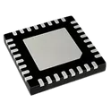
Maxim Integrated PLL Frequency Synthesizer Single 23.5MHz to 6000MHz 32-Pin TQFN EP QFN-32 Maxim None MAX2871ETJ+ Unavailable Maxim Integrated MAX2871 ultra-wideband fractional-N / integer-N PLL frequency synthesizer with integrated VCOs, capable of generating RF frequencies from 23.5MHz to 6.0GHz. Features programmable output dividers (1/2/4/8/16/32/64/128), dual differential RF outputs with programmable output power from -1dBm to +8dBm, low phase noise performance, phase frequency detector up to 140MHz, reference frequency up to 210MHz, fast lock and cycle-slip reduction, automatic/manual VCO selection, on-chip temperature sensor with 7-bit ADC, 4-wire SPI-compatible serial interface, and operation from -40°C to +85°C. Suitable for wireless infrastructure, clock generation, microwave radios, RF signal generation, and test & measurement equipment. MAX2871 Search Keywords: MAX2871, Maxim MAX2871, Analog Devices MAX2871, PLL synthesizer, RF synthesizer, fractional N synthesizer, integer N synthesizer, 6GHz frequency synthesizer, RF signal generator IC, integrated VCO synthesizer, microwave synthesizer, SPI frequency synthesizer, dual output PLL, clock generation IC, wireless infrastructure synthesizer Hashtags: #MAX2871 #MaximIntegrated #AnalogDevices #PLLSynthesizer #FrequencySynthesizer #RFSynthesizer #FractionalNPLL #IntegerNPLL #IntegratedVCO #RFSignalGenerator #MicrowaveRadio #ClockGeneration #WirelessInfrastructure #SPIInterface #TestAndMeasurement #RFDesign #RFIC #PhaseLockedLoop
0 Uses0 StarsADC09SJ1300AAVT
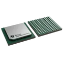
Analog to Digital Converters - ADC Single-channel, 9-bit, 1.3-GSPS analog-to-digital converter (ADC) with JESD204C interface 144-FCBGA -40 to 85 ADC09xJ1300 is a family of quad, dual and single channel, 9-bit, 1.3GSPS analog-to-digital converters (ADC). Low power consumption, high sampling rate and 9-bit resolution makes the ADC09xJ1300 ideally suited for suited for a variety of multi-channel communications and test systems. Full-power input bandwidth (-3dB) of 6GHz enables direct RF sampling of L-band and S-band. A number of clocking features are included to relax system hardware requirements, such as an internal phase-locked loop (PLL) with integrated voltagecontrolled oscillator (VCO) to generate the sampling clock. Four clock outputs are provided to clock the logic and SerDes of the FPGA or ASIC. A timestamp input and output is provided for pulsed systems. JESD204C serialized interface decreases system size by reducing the amount of printed circuit board (PCB) routing. Interface modes support from 2 to 8 lanes (dual and quad channel devices) or 1 to 4 lanes (for the single channel device), with SerDes baud-rates up to 17.16Gbps, to allow the optimal configuration for each application. Features • ADC Core: – Resolution: 9 Bit – Maximum sampling rate: 1.3GSPS – Non-interleaved architecture – Internal dither reduces high-order harmonics • Performance specifications (–1dBFS): – SNR (100 MHz): 53.5dBFS – ENOB (100 MHz): 8.5 Bits – SFDR (100 MHz): 64dBc – Noise floor (–20dBFS): –143dBFS • Full-scale input voltage: 80 mVPP-DIFF • Full-power input bandwidth: 6GHz • JESD204C Serial data interface: – Support for 2 to 8 (Quad/Dual channel) or 1 to 4 (Single channel) total SerDes lanes – Maximum baud-rate: 17.16Gbps – 64B/66B and 8B/10B encoding modes – Subclass-1 support for deterministic latency – Compatible with JESD204B receivers • Optional internal sampling clock generation – Internal PLL and VCO (7.2–8.2GHz) • SYSREF Windowing eases synchronization • Four clock outputs simplify system clocking – Reference clocks for FPGA or adjacent ADC – Reference clock for SerDes transceivers • Timestamp input and output for pulsed systems • Power consumption (1GSPS): – Quad Channel: 450mW / channel – Dual channel: 625mW / channel – Single channel: 940mW • Power supplies: 1.1V, 1.9V #CommonPartsLibrary #IntegratedCircuit #ADC #HighSpeedADC #RFADC #JESD204C #13GSPS #9bitADC #DirectRFSampling #TexasInstruments #MixedSignal #DataAcquisition #JESD204
0 Uses0 StarsADN4624BCPZ
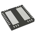
LVDS Digital Isolator 5700Vrms 4 Channel 2.5Gbps 40kV/µs CMTI 32-WFQFN Exposed Pad, CSP The ADN4624 is a quad-channel, signal isolated, low voltage differential signaling (LVDS) buffer that operates at up to 2.5 Gbps with very low jitter. The device integrates Analog Devices, Inc., iCoupler® technology, enhanced for high speed operation to provide drop-in galvanic isolation of LVDS signal chains. AC coupling and/or level shifting to the LVDS receivers and from the LVDS drivers allows isolation of other high speed signals such as current mode logic (CML). The ADN4624 includes a refresh mechanism to monitor the input and output states and ensure they remain the same in the absence of data transitions (for example, at power-on). For lower power consumption and high speed operation with low jitter, the LVDS and isolator circuits rely on 1.8 V supplies. The ADN4624 is fully specified over a wide industrial temperature range and is available in a 28-lead, wide-body, finer pitch SOIC_W_FP package with 8.3 mm creepage and clearance (for 5.7 kV rms or 8 kVPEAK surge and impulse voltages and reinforced insulation at ac mains voltages) or 6 mm × 6 mm LFCSP package with 1.27 mm creepage and clearance (for basic/functional isolation). FEATURES ► 5.7 kV rms and 1.5 kV rms LVDS isolators ► Complies with TIA/EIA-644-A LVDS signal levels ► Quad-channel configuration ► Any data rate up to 2.5 Gbps switching with low jitter ► 10 Gbps total bandwidth across four channels ► 2.15 ns typical propagation delay ► Typical jitter: 0.82 ps rms random, 40 ps total peak ► Lower power 1.8 V supplies ► ±8 kV IEC 61000-4-2 ESD protection across isolation barrier ► High common-mode transient immunity: 100 kV/μs typical ► Safety and regulatory approvals (28-lead SOIC_W_FP package) ► UL (pending): 5700 V rms for 1 minute per UL 1577 ► CSA Component Acceptance Notice 5A (pending) ► VDE certificate of conformity (pending) ► DIN V VDE V 0884-11 (VDE V 0884-11):2017-01 ► VIORM = 849 VPEAK (working voltage) ► Enable or disable refresh (low speed output correctness check) ► Operating temperature range: −40°C to +125°C ► 28-lead, wide-body, finer pitch SOIC_W_FP package with 8.3 mm creepage and clearance or 6 mm × 6 mm LFCSP package with 1.27 mm creepage and clearance APPLICATIONS ► Isolated video and imaging data ► Analog front-end isolation ► Data plane isolation ► Isolated high speed clock and data links ► Multi-gigabit serialization/deserialization (SERDES) ► Board-to-board optical replacement (for example, short reach fiber) #CommonPartsLibrary #Isolator #ADN4624BCPZ #AnalogDevices #LVDS #DigitalIsolator #GalvanicIsolation #HighSpeedCommunication #SERDES
0 Uses0 StarsADN4624BRNZ
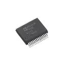
5.7 kV RMS/1.5 kV RMS, Quad-Channel LVDS 2.5 Gigabit Isolator (0 Reverse Channels) LVDS Digital Isolator 5700Vrms 4 Channel 2.5Gbps 40kV/µs CMTI 28-BSSOP (0.295", 7.50mm Width) The ADN4624 is a quad-channel, signal isolated, low voltage differential signaling (LVDS) buffer that operates at up to 2.5 Gbps with very low jitter. The device integrates Analog Devices, Inc., iCoupler® technology, enhanced for high speed operation to provide drop-in galvanic isolation of LVDS signal chains. AC coupling and/or level shifting to the LVDS receivers and from the LVDS drivers allows isolation of other high speed signals such as current mode logic (CML). The ADN4624 includes a refresh mechanism to monitor the input and output states and ensure they remain the same in the absence of data transitions (for example, at power-on). For lower power consumption and high speed operation with low jitter, the LVDS and isolator circuits rely on 1.8 V supplies. The ADN4624 is fully specified over a wide industrial temperature range and is available in a 28-lead, wide-body, finer pitch SOIC_W_FP package with 8.3 mm creepage and clearance (for 5.7 kV rms or 8 kVPEAK surge and impulse voltages and reinforced insulation at ac mains voltages) or 6 mm × 6 mm LFCSP package with 1.27 mm creepage and clearance (for basic/functional isolation). FEATURES ► 5.7 kV rms and 1.5 kV rms LVDS isolators ► Complies with TIA/EIA-644-A LVDS signal levels ► Quad-channel configuration ► Any data rate up to 2.5 Gbps switching with low jitter ► 10 Gbps total bandwidth across four channels ► 2.15 ns typical propagation delay ► Typical jitter: 0.82 ps rms random, 40 ps total peak ► Lower power 1.8 V supplies ► ±8 kV IEC 61000-4-2 ESD protection across isolation barrier ► High common-mode transient immunity: 100 kV/μs typical ► Safety and regulatory approvals (28-lead SOIC_W_FP package) ► UL (pending): 5700 V rms for 1 minute per UL 1577 ► CSA Component Acceptance Notice 5A (pending) ► VDE certificate of conformity (pending) ► DIN V VDE V 0884-11 (VDE V 0884-11):2017-01 ► VIORM = 849 VPEAK (working voltage) ► Enable or disable refresh (low speed output correctness check) ► Operating temperature range: −40°C to +125°C ► 28-lead, wide-body, finer pitch SOIC_W_FP package with 8.3 mm creepage and clearance or 6 mm × 6 mm LFCSP package with 1.27 mm creepage and clearance APPLICATIONS ► Isolated video and imaging data ► Analog front-end isolation ► Data plane isolation ► Isolated high speed clock and data links ► Multi-gigabit serialization/deserialization (SERDES) ► Board-to-board optical replacement (for example, short reach fiber) #CommonPartsLibrary #ADN4624BRNZ #DigitalIsolator #LVDS #AnalogDevices #HighSpeedInterface #GalvanicIsolation #LVDSIsolator #DigitalIsolation #IndustrialElectronics #HighSpeedData #SERDES #SignalIntegrity #EmbeddedSystems #ElectronicsDesign #InterfaceICs
0 Uses0 StarsRK809-5
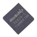
QFN-68-EP(7x7) Power Management - Specialized RoHS The RK809-5 is a highly integrated Power Management Integrated Circuit (PMIC) from Rockchip designed for multi-core processor systems and embedded applications. It provides a complete power management solution by integrating multiple high-efficiency DC-DC buck converters, LDO regulators, power sequencing logic, battery fuel gauging, RTC functionality, and audio codec capabilities into a single device. The RK809-5 is commonly used alongside Rockchip SoCs in single-board computers, tablets, AIoT devices, and industrial embedded systems. Key Features Five high-efficiency synchronous buck converters with fast transient response. Nine low-dropout (LDO) voltage regulators for powering sensitive analog and digital circuits. Integrated battery fuel gauge for battery capacity monitoring. Configurable power-up and power-down sequencing (OTP programmable). Dynamic Voltage Scaling (DVS/DVFS) support via I²C interface. Integrated Real-Time Clock (RTC) with 32.768 kHz crystal oscillator support. Two integrated load switches for peripheral power control. Over-current, over-voltage, and thermal protection features. Built-in audio CODEC with headphone driver and Class-D amplifier support. Designed to minimize external component count and simplify power system design. QFN-68-EP (7 mm × 7 mm) package. #RK8095 #RK809 #Rockchip #PMIC #PowerManagementIC #BatteryManagement #AudioCodec #RTC #DVFS #EmbeddedSystems #SingleBoardComputer #IoT #IndustrialElectronics #PowerSupplyDesign #ElectronicsEngineering
6 Uses0 StarsADF4351BCPZ
Clock Generators, PLLs, Frequency Synthesizers ADF4351BCPZ LFCSP-32_L5.0-W5.0-P0.50-BL-EP3.5 LCSC Part Number: C654681 JLCPCB Part Class: Extended Part Manufactured by ADI(亚德诺)/LINEAR(凌特) Analog Devices ADF4351 wideband fractional-N and integer-N PLL frequency synthesizer with integrated voltage-controlled oscillator (VCO), generating RF output frequencies from 35MHz to 4.4GHz. Features low phase noise, programmable output divider ratios (/1, /2, /4, /8, /16, /32, /64), programmable RF output power, dual-modulus prescaler (4/5 or 8/9), analog and digital lock detect, fast lock mode, cycle slip reduction, auxiliary RF output, RF mute function, and 3-wire serial programming interface. Operates from 3.0V to 3.6V and is widely used in RF signal generators, local oscillators, SDR systems, wireless infrastructure, test equipment, microwave communications, clock generation, and laboratory instrumentation. Search Keywords: ADF4351, Analog Devices ADF4351, ADF4351BRUZ, RF synthesizer, PLL synthesizer, fractional N PLL, integer N PLL, integrated VCO, 35MHz to 4.4GHz synthesizer, RF signal generator IC, microwave frequency synthesizer, local oscillator PLL, SDR synthesizer, programmable RF generator, low phase noise synthesizer, SPI PLL synthesizer, RF clock generator Hashtags: #ADF4351 #AnalogDevices #PLL #FractionalNPLL #IntegerNPLL #FrequencySynthesizer #RFSynthesizer #IntegratedVCO #RFGenerator #SignalGenerator #LocalOscillator #MicrowaveRF #SDR #ClockGenerator #RFIC #WirelessInfrastructure #TestEquipment #LowPhaseNoise #SPIInterface #ADF4351Module
31 Uses0 Stars