Switches
A switch is a device that allows electricity to flow through a circuit by completing or interrupting the connection. It is a common component in electrical and electronic systems and is used in a variety of applications, such as controlling the flow of electricity in a circuit, turning devices on and off, and routing electrical signals. One of the primary use cases for switches is to control the flow of electricity in a circuit. This can be done by manually flipping the switch or by using a control mechanism, such as a timer or a sensor. Another common use for switches is to turn devices on and off. This can be done using a switch that is built into the device or by using a separate switch that is connected to the device. In addition to these basic use cases, switches can also be used to route electrical signals. For example, a switch can be used to route a signal from one device to another or to direct a signal to a specific circuit or component. If you're looking for a wide variety of switches for your projects, flux.ai has the world's largest community-driven public library of them. The library includes footprints, symbols, datasheets, and simulation models for a wide range of switches, making it easy to find the right switch for your needs.
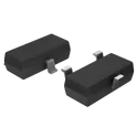
IRLML6244TRPBF
MOSFET N-CH 20V 6.3A SOT-23 The IRLML6244TRPBF is an N-channel enhancement-mode power MOSFET from Infineon Technologies (originally International Rectifier HEXFET series). It is designed for low-voltage power switching applications such as load switching, DC-DC converters, and LED control. It comes in a compact SOT-23 (Micro3™) surface-mount package, making it suitable for space-constrained PCB designs while still handling relatively high current for its size. Key Features Drain-Source Voltage (VDS): 20 V Continuous Drain Current: up to ~6.3 A (at 25°C) Very low RDS(on): ~21 mΩ @ VGS = 4.5 V ~27 mΩ @ VGS = 2.5 V Low gate threshold voltage (~0.5–1.1 V typical range) (note: not a switching guarantee) Gate-to-source voltage rating: ±12 V Low power loss due to low on-resistance High efficiency switching for low-voltage systems Power dissipation: ~1.3 W (thermal limited in SOT-23 package) Fast switching performance (low gate charge ~8.9 nC) Operating temperature range: −55°C to +150°C RoHS compliant (lead-free, halogen-free) Typical Applications Low-side load switching (MCUs, GPIO control) LED strip / RGB LED drivers Battery-powered systems DC-DC converter switching Small motor or relay driving General-purpose power management in compact electronics Important Design Note Even though it has a low VGS(th), this MOSFET is not selected based on threshold voltage. What matters is the RDS(on) at your gate drive voltage (2.5 V / 3.3 V / 5 V) to ensure it fully turns on with minimal heating. #CommonPartsLibrary #Transistor #FET #IRLML6244 #MOSFET #NChannelMOSFET #PowerElectronics #SOT23 #Infineon #HEXFET #LEDDriver #LowSideSwitch #ElectronicsComponents
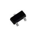
217 Uses0 StarsIRLML2502
MOSFET N-CH 20V 3.6A SOT-23 The IRLML2502 is a small-signal N-channel enhancement mode power MOSFET designed for low-voltage, high-efficiency switching applications. It is commonly used as a load switch or power control transistor in compact electronic systems such as battery-powered devices, LED drivers, and DC-DC converters. It features a low on-resistance (RDS(on)), which allows it to switch higher currents with minimal power loss and heat generation. The device is optimized for logic-level gate drive, meaning it can be driven directly from microcontrollers (like 3.3 V or 5 V systems). It is packaged in a compact SOT-23 (Micro3) surface-mount package, making it suitable for space-constrained PCB designs. Key Features N-channel enhancement mode MOSFET Drain-source voltage (VDS) up to 20 V Continuous drain current up to ~4.2 A (at 25°C) Very low RDS(on) ≈ 45 mΩ @ VGS = 4.5 V Logic-level gate drive capability (works with 2.5–4.5 V signals) Fast switching performance Compact SOT-23 (Micro3) surface-mount package Low gate charge for efficient switching Suitable for battery-powered and low-voltage applications RoHS compliant, lead-free design #IRLML2502 #MOSFET #NChannelMOSFET #PowerElectronics #SOT23 #LogicLevelMOSFET #PowerSwitch #ElectronicComponents #EmbeddedSystems #PCBDesign
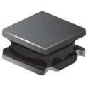
326 Uses0 StarsSRN3015-6R8M
Bourns SRN3015 Series semi-shielded power inductor, compact 3.0mm × 3.0mm × 1.5mm SMD package, ferrite core construction, inductance range 1.0µH to 100µH, rated current up to 2.35A, saturation current up to 2.35A, low DCR design, operating temperature -40°C to +125°C, RoHS compliant and halogen-free, optimized for DC/DC converters, portable electronics, digital cameras, HDDs, smartphones, LCD displays and compact power management applications. Search Keywords: SRN3015, Bourns SRN3015, SRN3015 power inductor, semi shielded inductor, SMD power inductor, 3x3mm inductor, ferrite inductor, DC DC converter inductor, low profile inductor, SRN3015-1R0Y, SRN3015-2R2M, SRN3015-4R7M, SRN3015-100M, power choke, switching regulator inductor Hashtags: #SRN3015 #BournsSRN3015 #Bourns #PowerInductor #SemiShieldedInductor #SMDInductor #FerriteInductor #DCDCInductor #SwitchingRegulatorInductor #PowerChoke #LowProfileInductor #3x3mmInductor #PortablePower #SMPSInductor #MagneticComponent
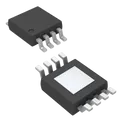
2 Uses0 StarsMP1584EN-LF-Z
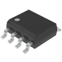
Buck Switching Regulator IC Positive Adjustable 0.8V 1 Output 3A 8-SOIC (0.154", 3.90mm Width) Exposed Pad MP1584EN-SOP8 MP1584EN-LF-Z is a high-frequency, non-synchronous step-down (buck) DC-DC switching regulator from Monolithic Power Systems. It integrates a high-side power MOSFET and is designed to efficiently convert input voltages from 4.5V to 28V into a lower, regulated output voltage with up to 3A output current. Its high switching frequency enables the use of small external components, making it ideal for compact and cost-effective power supply designs. Key Features: • Wide 4.5V to 28V input voltage range • Adjustable output voltage from 0.8V to 25V • Up to 3A continuous output current • Integrated high-side power MOSFET • Programmable switching frequency from 100kHz to 1.5MHz • Current-mode control for fast transient response • High efficiency with pulse-skipping mode at light loads • Low quiescent current operation • Internal soft-start function • Over-current and thermal shutdown protection • Stable with ceramic output capacitors • Available in SOIC-8E package with exposed thermal pad #MP1584EN #BuckConverter #DCDCConverter #SwitchingRegulator #PowerManagement #VoltageRegulator #MPS #MonolithicPowerSystems #EmbeddedSystems #ElectronicsDesign #PowerSupply #PCBDesign #HardwareEngineering #Electronics #Semiconductor #power #PMIC #IC
165 Uses0 StarsADN4624BCPZ
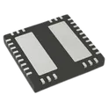
LVDS Digital Isolator 5700Vrms 4 Channel 2.5Gbps 40kV/µs CMTI 32-WFQFN Exposed Pad, CSP The ADN4624 is a quad-channel, signal isolated, low voltage differential signaling (LVDS) buffer that operates at up to 2.5 Gbps with very low jitter. The device integrates Analog Devices, Inc., iCoupler® technology, enhanced for high speed operation to provide drop-in galvanic isolation of LVDS signal chains. AC coupling and/or level shifting to the LVDS receivers and from the LVDS drivers allows isolation of other high speed signals such as current mode logic (CML). The ADN4624 includes a refresh mechanism to monitor the input and output states and ensure they remain the same in the absence of data transitions (for example, at power-on). For lower power consumption and high speed operation with low jitter, the LVDS and isolator circuits rely on 1.8 V supplies. The ADN4624 is fully specified over a wide industrial temperature range and is available in a 28-lead, wide-body, finer pitch SOIC_W_FP package with 8.3 mm creepage and clearance (for 5.7 kV rms or 8 kVPEAK surge and impulse voltages and reinforced insulation at ac mains voltages) or 6 mm × 6 mm LFCSP package with 1.27 mm creepage and clearance (for basic/functional isolation). FEATURES ► 5.7 kV rms and 1.5 kV rms LVDS isolators ► Complies with TIA/EIA-644-A LVDS signal levels ► Quad-channel configuration ► Any data rate up to 2.5 Gbps switching with low jitter ► 10 Gbps total bandwidth across four channels ► 2.15 ns typical propagation delay ► Typical jitter: 0.82 ps rms random, 40 ps total peak ► Lower power 1.8 V supplies ► ±8 kV IEC 61000-4-2 ESD protection across isolation barrier ► High common-mode transient immunity: 100 kV/μs typical ► Safety and regulatory approvals (28-lead SOIC_W_FP package) ► UL (pending): 5700 V rms for 1 minute per UL 1577 ► CSA Component Acceptance Notice 5A (pending) ► VDE certificate of conformity (pending) ► DIN V VDE V 0884-11 (VDE V 0884-11):2017-01 ► VIORM = 849 VPEAK (working voltage) ► Enable or disable refresh (low speed output correctness check) ► Operating temperature range: −40°C to +125°C ► 28-lead, wide-body, finer pitch SOIC_W_FP package with 8.3 mm creepage and clearance or 6 mm × 6 mm LFCSP package with 1.27 mm creepage and clearance APPLICATIONS ► Isolated video and imaging data ► Analog front-end isolation ► Data plane isolation ► Isolated high speed clock and data links ► Multi-gigabit serialization/deserialization (SERDES) ► Board-to-board optical replacement (for example, short reach fiber) #CommonPartsLibrary #Isolator #ADN4624BCPZ #AnalogDevices #LVDS #DigitalIsolator #GalvanicIsolation #HighSpeedCommunication #SERDES
0 Uses0 StarsADN4624BRNZ
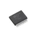
5.7 kV RMS/1.5 kV RMS, Quad-Channel LVDS 2.5 Gigabit Isolator (0 Reverse Channels) LVDS Digital Isolator 5700Vrms 4 Channel 2.5Gbps 40kV/µs CMTI 28-BSSOP (0.295", 7.50mm Width) The ADN4624 is a quad-channel, signal isolated, low voltage differential signaling (LVDS) buffer that operates at up to 2.5 Gbps with very low jitter. The device integrates Analog Devices, Inc., iCoupler® technology, enhanced for high speed operation to provide drop-in galvanic isolation of LVDS signal chains. AC coupling and/or level shifting to the LVDS receivers and from the LVDS drivers allows isolation of other high speed signals such as current mode logic (CML). The ADN4624 includes a refresh mechanism to monitor the input and output states and ensure they remain the same in the absence of data transitions (for example, at power-on). For lower power consumption and high speed operation with low jitter, the LVDS and isolator circuits rely on 1.8 V supplies. The ADN4624 is fully specified over a wide industrial temperature range and is available in a 28-lead, wide-body, finer pitch SOIC_W_FP package with 8.3 mm creepage and clearance (for 5.7 kV rms or 8 kVPEAK surge and impulse voltages and reinforced insulation at ac mains voltages) or 6 mm × 6 mm LFCSP package with 1.27 mm creepage and clearance (for basic/functional isolation). FEATURES ► 5.7 kV rms and 1.5 kV rms LVDS isolators ► Complies with TIA/EIA-644-A LVDS signal levels ► Quad-channel configuration ► Any data rate up to 2.5 Gbps switching with low jitter ► 10 Gbps total bandwidth across four channels ► 2.15 ns typical propagation delay ► Typical jitter: 0.82 ps rms random, 40 ps total peak ► Lower power 1.8 V supplies ► ±8 kV IEC 61000-4-2 ESD protection across isolation barrier ► High common-mode transient immunity: 100 kV/μs typical ► Safety and regulatory approvals (28-lead SOIC_W_FP package) ► UL (pending): 5700 V rms for 1 minute per UL 1577 ► CSA Component Acceptance Notice 5A (pending) ► VDE certificate of conformity (pending) ► DIN V VDE V 0884-11 (VDE V 0884-11):2017-01 ► VIORM = 849 VPEAK (working voltage) ► Enable or disable refresh (low speed output correctness check) ► Operating temperature range: −40°C to +125°C ► 28-lead, wide-body, finer pitch SOIC_W_FP package with 8.3 mm creepage and clearance or 6 mm × 6 mm LFCSP package with 1.27 mm creepage and clearance APPLICATIONS ► Isolated video and imaging data ► Analog front-end isolation ► Data plane isolation ► Isolated high speed clock and data links ► Multi-gigabit serialization/deserialization (SERDES) ► Board-to-board optical replacement (for example, short reach fiber) #CommonPartsLibrary #ADN4624BRNZ #DigitalIsolator #LVDS #AnalogDevices #HighSpeedInterface #GalvanicIsolation #LVDSIsolator #DigitalIsolation #IndustrialElectronics #HighSpeedData #SERDES #SignalIntegrity #EmbeddedSystems #ElectronicsDesign #InterfaceICs
0 Uses0 StarsRK809-5
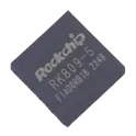
Rockchip RK809 highly integrated PMIC with audio codec for multi-core system applications, providing five configurable synchronous step-down converters, nine LDO regulators, two switches, battery fuel gauge, configurable power-up/power-down sequencing, integrated RTC with 32.768kHz clock support, I2C interface for voltage and fuel gauge control, dynamic DC/DC output voltage adjustment, soft-start on all channels, 2MHz switching frequency, integrated power switches, headphone driver and Class-D audio driver, QFN68 7.0 x 7.0mm package. Search Keywords: RK809, Rockchip RK809, RK809 PMIC, RK809 power management IC, RK809 codec PMIC, RK809 battery fuel gauge, RK809 audio codec, RK809 DC DC converter, RK809 LDO regulator, RK809 I2C PMIC, RK809 RTC, RK809 QFN68, Rockchip PMIC, RK809 datasheet Hashtags: #RK809 #RockchipRK809 #RockchipPMIC #PMIC #PowerManagementIC #AudioCodecPMIC #BatteryFuelGauge #DCDCConverter #LDORegulator #I2CPMIC #RTC #ClassDAudio #QFN68
1 Uses0 StarsRK809-5
QFN-68-EP(7x7) Power Management - Specialized RoHS The RK809-5 is a highly integrated Power Management Integrated Circuit (PMIC) from Rockchip designed for multi-core processor systems and embedded applications. It provides a complete power management solution by integrating multiple high-efficiency DC-DC buck converters, LDO regulators, power sequencing logic, battery fuel gauging, RTC functionality, and audio codec capabilities into a single device. The RK809-5 is commonly used alongside Rockchip SoCs in single-board computers, tablets, AIoT devices, and industrial embedded systems. Key Features Five high-efficiency synchronous buck converters with fast transient response. Nine low-dropout (LDO) voltage regulators for powering sensitive analog and digital circuits. Integrated battery fuel gauge for battery capacity monitoring. Configurable power-up and power-down sequencing (OTP programmable). Dynamic Voltage Scaling (DVS/DVFS) support via I²C interface. Integrated Real-Time Clock (RTC) with 32.768 kHz crystal oscillator support. Two integrated load switches for peripheral power control. Over-current, over-voltage, and thermal protection features. Built-in audio CODEC with headphone driver and Class-D amplifier support. Designed to minimize external component count and simplify power system design. QFN-68-EP (7 mm × 7 mm) package. #RK8095 #RK809 #Rockchip #PMIC #PowerManagementIC #BatteryManagement #AudioCodec #RTC #DVFS #EmbeddedSystems #SingleBoardComputer #IoT #IndustrialElectronics #PowerSupplyDesign #ElectronicsEngineering
6 Uses0 StarsXL6007E1
The XL6007 regulator is a wide input range, current mode, DC/DC converter which is capable of generating either positive or negative output voltages. It can be configured as either a boost, flyback, SEPIC or inverting converter. The XL6007 built in N-channel power MOSFET and fixed frequency oscillator, current-mode architecture results in stable operation over a wide range of supply and output voltages. The XL6007 regulator is special design for portable electronic equipment. Wide 3.6V to 24V Input Voltage Range Positive or Negative Output Voltage Programming with a Single Feedback Pin Current Mode Control Provides Excellent Transient Response 1.25V reference adjustable version Fixed 400KHz Switching Frequency Maximum 2A Switching Current SW PIN Built in Over Voltage Protection Excellent line and load regulation EN PIN TTL shutdown capability Internal Optimize Power MOSFET High efficiency up to 90% Built in Frequency Compensation Built in Soft-Start Function Built in Thermal Shutdown Function Built in Current Limit Function Available in SOP8 package Applications Automotive and Industrial Boost / Buck-Boost / Inverting Converters Portable Electronic Equipment #commonpartslibrary #integratedcircuit
0 Uses0 Stars