Switches
A switch is a device that allows electricity to flow through a circuit by completing or interrupting the connection. It is a common component in electrical and electronic systems and is used in a variety of applications, such as controlling the flow of electricity in a circuit, turning devices on and off, and routing electrical signals. One of the primary use cases for switches is to control the flow of electricity in a circuit. This can be done by manually flipping the switch or by using a control mechanism, such as a timer or a sensor. Another common use for switches is to turn devices on and off. This can be done using a switch that is built into the device or by using a separate switch that is connected to the device. In addition to these basic use cases, switches can also be used to route electrical signals. For example, a switch can be used to route a signal from one device to another or to direct a signal to a specific circuit or component. If you're looking for a wide variety of switches for your projects, flux.ai has the world's largest community-driven public library of them. The library includes footprints, symbols, datasheets, and simulation models for a wide range of switches, making it easy to find the right switch for your needs.
MPL-AY1265-2R2
2.2µH Unshielded Molded Inductor 17 A 3.7mOhm 2-SMD, J-Lead The MPL-AY1265-2R2 is a 2.2 µH surface-mount molded power inductor from Monolithic Power Systems (MPS). It is designed for high-current DC-DC switching power supplies and power management applications requiring low DC resistance (DCR), high efficiency, and stable inductance over a wide operating temperature range. Its molded construction minimizes audible noise and provides excellent mechanical reliability for compact, high-performance electronic designs. Key Features 2.2 µH inductance with ±20% tolerance High rated current: up to 17 A Low DC resistance: 3.7 mΩ typ. (4.3 mΩ max.) Soft saturation characteristics for improved reliability Molded construction for enhanced durability and reduced EMI Low audible noise during switching operation Stable performance across a wide temperature range Operating temperature: −40°C to +155°C Compact SMD package: 13.5 × 12.6 × 6.2 mm RoHS/REACH compliant and halogen-free Typical Applications Battery-powered devices Portable electronics Embedded computing systems High-current switching mode power supplies (SMPS) High-frequency DC-DC converters Point-of-load (POL) converters FPGA power rails #MoldedInductor #PowerInductor #2_2uH #HighCurrent #LowDCR #SMPS #DCDCConverter #PowerManagement #SMD #MonolithicPowerSystems #RoHS #EmbeddedSystems
4 Uses0 Stars2961299
REL-MR- 12DC/21-21AU - Plug-in miniature power relay, with multi-layer gold contact, 2 changeover contacts, input voltage 12 V DC General Purpose Relay DPDT (2 Form C) 12VDC Coil Through Hole The Phoenix Contact 2961299 (REL-MR-12DC/21-21AU) is a plug-in miniature power relay designed for reliable switching in industrial automation, control panels, and interface applications. It features a 12 VDC monostable coil, 2 changeover (DPDT) contacts, and hard gold-plated AgNi contacts, making it suitable for switching low-level signals with high reliability. The relay is RT III sealed (wash-proof), ensuring protection against contaminants during PCB cleaning and harsh industrial environments. It is intended for use with compatible Phoenix Contact relay bases and accessories. Key Features 12 VDC monostable coil operation 2 changeover (DPDT) contacts Hard gold-plated AgNi contacts for reliable low-level signal switching RT III sealed (wash-proof) construction Mechanical life: up to 30 million operations 5 kV coil-to-contact isolation Fast operate and release times (typ. 7 ms / 3 ms) Designed for industrial control, PLC interfaces, automation, and switching applications Compatible with Phoenix Contact relay sockets and interface modules #PhoenixContact #Relay #PowerRelay #DPDTRelay #IndustrialAutomation #ControlPanel #PLC #InterfaceRelay #12VDC #ElectromechanicalRelay
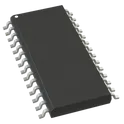
4 Uses0 StarsLT3641EFE#PBF
Buck Switching Regulator IC Positive Adjustable 0.6V, 1.265V 2 Output 1.3A, 1.1A 28-TSSOP (0.173", 4.40mm Width) Exposed Pad The LT3641EFE#PBF specification defines the engineering requirements for a dual-channel step-down switching regulator integrated circuit designed for high-efficiency power conversion and distribution applications. This specification establishes the functional, electrical, mechanical, thermal, environmental, and quality requirements necessary to ensure stable voltage regulation, efficient power delivery, and long-term operational reliability in industrial, embedded, communication, and control systems. The device is intended for use in distributed power architectures, industrial automation equipment, instrumentation, telecommunications systems, automotive electronics, and embedded applications requiring multiple regulated output voltages from a common input source. The integrated dual-channel architecture enables compact power supply designs while providing high conversion efficiency, low power dissipation, and reliable performance across a wide range of operating conditions. Engineering Requirements The switching regulator shall be manufactured using qualified semiconductor fabrication processes and high-quality materials to ensure consistent electrical performance, efficient power conversion, and dependable long-term reliability. The device shall maintain stable operation under specified input voltage, output load, temperature, and environmental operating conditions. Electrical characteristics shall provide accurate output voltage regulation, high conversion efficiency, low output ripple, and fast transient response. The regulator shall maintain stable switching behavior during startup, shutdown, load variations, and input voltage fluctuations while ensuring reliable power delivery to connected circuits. The integrated control architecture shall support independent regulation of multiple output channels and provide reliable operation during dynamic system conditions. Built-in protection functions shall support safe operation during abnormal events including overload, short-circuit, thermal stress, and fault conditions, thereby enhancing overall system reliability. Thermal performance shall support continuous operation within the specified junction temperature range while maintaining electrical integrity and long-term reliability. The package shall facilitate effective heat dissipation and shall be suitable for automated surface-mount assembly and standard solder reflow manufacturing processes. Mechanical construction shall withstand thermal cycling, vibration, mechanical handling, and environmental exposure without degradation of electrical or structural performance. Workmanship shall be free from defects including contamination, package cracking, bond failures, lead deformation, or structural inconsistencies that could adversely affect functionality or reliability. Inspection, validation, and testing shall be performed using calibrated equipment and controlled quality procedures to verify compliance with engineering and manufacturing requirements. Any deviation from this specification shall require formal engineering evaluation, documented technical justification, and approval through the established engineering change control process before implementation. Documentation Supporting documentation shall include engineering drawings, electrical performance specifications, thermal characterization reports, application guidelines, qualification records, inspection reports, reliability data, material declarations, and revision-controlled manufacturing documentation. All documentation shall be maintained under formal configuration management and quality assurance systems to ensure complete product traceability. Revision Control Any modification to this specification shall be managed through the formal engineering change management process. All revisions shall undergo technical review, validation, and approval before release to ensure continued compliance with design intent and applicable engineering standards. #EngineeringSpecification #SwitchingRegulator #BuckConverter #PowerManagement #DCDCConverter #PowerElectronics #EmbeddedSystems #IndustrialElectronics #QualityAssurance #EngineeringDocumentation
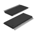
0 Uses0 StarsSN74CBT16390DL
Multiplexer/Demultiplexer 16 x 1:2 56-SSOP The SN74CBT16390 is a 16-bit to 32-bit switch used in applications in which two separate data paths must be multiplexed onto, or demultiplexed from, a single path. This device can be used for memory interleaving, in which two different banks of memory must be addressed simultaneously. This device also can be used to connect or isolate the PCI bus to one or two slots simultaneously. Two output enables (OE1 and OE2) control the data flow. When OE1 is low, A port is connected to 1B port. When OE2 is low, A port is connected to 2B port. When both OE1 and OE2 are low, the A port is connected to both 1B and 2B ports. The control inputs can be driven with a 5-V CMOS, 5-V TTL, or an LVTTL driver. Key Features 16-bit to 32-bit FET multiplexer/demultiplexer bus switch Operates from 4.5 V to 5.5 V Low ON-state resistance for high-speed signal switching Near-zero propagation delay through the switch Dual output-enable (OE1, OE2) controls for flexible routing TTL-compatible control inputs Supports memory interleaving and PCI bus applications Low power consumption ESD protection compliant with JESD22 standards Operating temperature range: −40°C to +85°C Available in a 56-pin SSOP (DL) package #BusSwitch #Multiplexer #Demultiplexer #Widebus #DigitalLogic #HighSpeedInterface #MemoryInterleaving #PCIBus #TexasInstruments #SN74CBT16390 #SSOP56
0 Uses0 StarsEPC2019
GANFET N-CH 200V 8.5A DIE The EPC2019 is an enhancement-mode N-channel Gallium Nitride (eGaN®) power transistor designed for high-speed and high-efficiency power conversion applications. With a 200 V drain-to-source voltage rating, 42 mΩ maximum RDS(on), and 8.5 A continuous drain current, it offers significantly lower switching losses than conventional silicon MOSFETs. Its ultra-low gate charge, zero reverse recovery charge (QRR), and fast switching characteristics make it ideal for high-frequency switching circuits. The device is supplied in a bare die (passivated die with solder bars) package for optimized thermal and electrical performance in compact, high-density designs. Key Features Enhancement-mode N-channel eGaN® FET 200 V drain-to-source voltage (VDS) 42 mΩ maximum RDS(on) @ VGS = 5 V 8.5 A continuous drain current Ultra-low gate charge (Qg ≈ 2.9 nC) Zero reverse recovery charge (QRR) for reduced switching losses Supports high-frequency switching operation Gate drive compatible with 0 V OFF / 5 V ON (no negative gate voltage required) Bare die package for compact, high-performance power designs Operating junction temperature: −40°C to +150°C #EPC2019 #eGaN #GaNFET #PowerTransistor #NChannelFET #HighEfficiency #HighSpeedSwitching #PowerElectronics #DCDCConverter #ClassDAudio #EfficientPowerConversion
6 Uses0 StarsTS5A23157RSER
2 Circuit IC Switch 2:1 10Ohm 10-UQFN (2.0x1.5) The TS5A23157 device is a dual single-pole doublethrow (SPDT) analog switch designed to operate from 1.65 V to 5.5 V. This device can handle both digital and analog signals. Signals up to 5.5 V (peak) can be transmitted in either direction. Features 1• Low ON-State Resistance (15 Ω at 125℃) • 125℃ Operation • Control Inputs are 5-V Tolerant • Specified Break-Before-Make Switching • Low Charge Injection • Excellent ON-Resistance Matching • Low Total Harmonic Distortion • 1.8-V to 5.5-V Single-Supply Operation • Latch-Up Performance Exceeds 100 mA Per JESD 78, Class II • ESD Performance Tested Per JESD 22 – 2000-V Human-Body Model (A114-B, Class II) – 1000-V Charged-Device Model (C101) 2 Applications • Sample-and-Hold Circuits • Battery-Powered Equipment • Audio and Video Signal Routing • Communication Circuits #commonpartslibrary #integratedcircuit #circuitswitch #TexasInstruments #AnalogSwitch #SPDT #SignalRouting #Multiplexer #LowOnResistance #HighSpeedSwitching #UQFN #EmbeddedSystems #ElectronicsDesign
13 Uses0 Stars