Interface ICs
An interface IC is a type of integrated circuit that is designed to facilitate communication between two devices or systems. These devices are commonly used in electronic systems to enable the transfer of data and control signals between different components or subsystems. Some common use cases for interface ICs include connecting microcontrollers to peripherals such as sensors or displays, linking multiple processors together in a network, and enabling communication between devices using different communication protocols. Flux.ai has the world's largest community-driven public library of interface ICs, with footprints, symbols, datasheets, and simulation models. This library is a valuable resource for engineers and designers who need access to accurate and up-to-date information on these important components. Whether you are working on a new design project or simply looking to learn more about interface ICs, Flux.ai is an excellent resource to help you find the information you need.
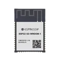
ESP32-S3-WROOM-1-N8
ESP32-S3-WROOM-1-N8 is a high-performance Wi-Fi and Bluetooth Low Energy (BLE) module from Espressif Systems. It is built around the ESP32-S3 SoC, featuring a dual-core Xtensa LX7 processor, integrated 2.4 GHz Wi-Fi and Bluetooth 5 LE connectivity, 8 MB SPI flash memory, and a PCB antenna. The module is optimized for AIoT, edge computing, human-machine interfaces, smart devices, and industrial IoT applications. Key Features Dual-core Xtensa® LX7 CPU running up to 240 MHz for high-performance embedded applications. 8 MB onboard SPI Flash (N8 variant) for firmware and data storage. 2.4 GHz Wi-Fi (802.11 b/g/n) with data rates up to 150 Mbps. Bluetooth 5 LE support including: Long Range mode 2 Mbps PHY Bluetooth Mesh Extended Advertising AI acceleration support through ESP32-S3 vector instructions for machine learning and signal-processing workloads. USB 1.1 OTG and USB Serial/JTAG integrated, simplifying debugging and USB device applications. Up to 45 GPIOs with extensive peripheral support: SPI I²C I²S UART PWM ADC Touch Sensors TWAI® (CAN-compatible) Camera Interface LCD Interface SDIO Host MCPWM Integrated 40 MHz crystal oscillator, RF matching circuitry, and PCB antenna for reduced external component count. Operating voltage range: 3.0 V to 3.6 V. Compact surface-mount module suitable for space-constrained designs. Typical Applications Smart home and home automation devices HMI displays and touchscreen products Voice recognition and audio processing Edge AI and machine learning applications Industrial IoT gateways and sensors Video streaming and camera systems USB-connected embedded devices Smart agriculture and healthcare equipment N8 specifically indicates 8 MB Flash and no PSRAM, making it a good choice for applications requiring substantial program storage but not large external RAM. #RF-transceiver #Module #ESP32
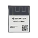
235 Uses0 StarsESP32-C3-MINI-1-H4
ESP32-C3-MINI-1-H4 is a compact, low-power wireless module from Espressif Systems built around the ESP32-C3 SoC. It integrates a 32-bit RISC-V processor, 2.4 GHz Wi-Fi, Bluetooth 5 LE, onboard 4 MB flash memory, crystal oscillator, RF matching circuitry, and a PCB antenna in a small surface-mount package. The module is designed for IoT devices, smart home products, industrial automation, wearable electronics, and wireless sensor applications. Key Features 32-bit RISC-V single-core processor with clock speeds up to 160 MHz. 2.4 GHz Wi-Fi 4 (802.11 b/g/n) connectivity. Bluetooth 5 Low Energy (BLE 5.0) support with long-range capability. 4 MB embedded SPI flash memory (H4 variant). 384 KB ROM and 408 KB SRAM for application execution. Integrated PCB antenna for simplified RF design. USB Serial/JTAG controller for programming and debugging without an external USB-to-UART bridge. Multiple peripheral interfaces: UART SPI I²C I²S PWM GPIO ADC USB JTAG Operating voltage range: 3.0 V to 3.6 V. Supports secure boot, flash encryption, and hardware cryptographic acceleration. Compact SMD module suitable for space-constrained designs. Typical Applications Smart home and home automation devices Wireless sensors and data loggers IoT gateways and edge devices Industrial monitoring and control systems Bluetooth beacons Wearable electronics Consumer connected products H4 Variant Note: The ESP32-C3-MINI-1-H4 version includes 4 MB flash memory and supports an extended operating temperature range up to 105°C, making it suitable for more demanding industrial environments. #RF-Transceiver #ESP32 #Module
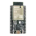
99 Uses0 StarsESP32-DevKitC
The ESP32-DevKitC is an official ESP32-based development board from Espressif Systems designed for rapid prototyping and IoT application development. It integrates an ESP32 module (such as ESP32-WROOM-32E or ESP32-WROVER variants), USB-to-UART programming interface, power regulation circuitry, reset and boot buttons, and access to most ESP32 GPIOs through dual-row headers. The board is breadboard-friendly and supports wireless connectivity, making it suitable for smart devices, industrial monitoring, home automation, wearable electronics, and embedded control systems. Key Features ESP32 Dual-Core Processor Xtensa® 32-bit LX6 dual-core MCU Up to 240 MHz clock frequency High-performance embedded processing capability. Wireless Connectivity Integrated 2.4 GHz Wi-Fi (802.11 b/g/n) Bluetooth Classic (BR/EDR) and Bluetooth Low Energy (BLE) support. Memory Typically includes 4 MB SPI Flash Some variants provide additional PSRAM for memory-intensive applications. Rich Peripheral Interfaces UART, SPI, I²C, I²S, SDIO ADC and DAC PWM outputs Capacitive touch sensing Pulse counter and timer peripherals. Extensive GPIO Access Most ESP32 pins are broken out to headers Supports digital I/O, interrupts, analog inputs, and communication interfaces. Development-Friendly Hardware USB-to-UART bridge for programming and debugging Dedicated EN (Reset) and BOOT buttons On-board 3.3 V regulator Breadboard-compatible layout. Flexible Power Options Powered through Micro-USB and onboard power circuitry Supports external power connections through header pins. #DevelopmentBoard
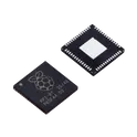
179 Uses0 StarsRP2040
133MHz LQFN-56(7x7) Microcontrollers (MCU/MPU/SOC) ROHS RP2040 The RP2040 is a high-performance, low-cost 32-bit microcontroller developed by Raspberry Pi Ltd.. It features dual ARM Cortex-M0+ processor cores, flexible digital interfaces, and a unique Programmable I/O (PIO) subsystem that enables custom hardware protocols and timing-critical applications. The device is widely used in embedded systems, IoT devices, robotics, industrial control, consumer electronics, and educational projects. Key Features Dual ARM Cortex-M0+ CPU cores operating up to 133 MHz (up to 200 MHz under specific conditions) 264 KB on-chip SRAM organized in six independent memory banks External QSPI Flash interface with Execute-In-Place (XIP) support and up to 16 MB Flash memory capability 30 multifunction GPIO pins with extensive peripheral multiplexing 2 × UART interfaces 2 × SPI controllers 2 × I²C controllers 16 PWM channels for motor control and signal generation USB 1.1 Host and Device support with integrated PHY 12-bit ADC with four external analog inputs and internal temperature sensor, up to 500 ksps sampling rate 12-channel DMA controller for efficient data transfers Programmable I/O (PIO) subsystem with 8 state machines for implementing custom communication interfaces and precise timing applications Integrated PLLs and programmable LDO regulator for clock and power management Operating voltage range: 1.8 V to 3.3 V Available in a compact 7 mm × 7 mm QFN-56 package Typical Applications IoT and connected devices Industrial automation Robotics and motor control Human-machine interfaces (HMI) Consumer electronics USB peripherals Sensor data acquisition systems Educational and maker projects Custom communication protocol implementations using PIO #CommonPartsLibrary #IntegratedCircuit #Microcontroller
129 Uses0 StarsSTUSB4500QTR
USB Controller USB 2.0 I2C Interface 24-QFN (4x4) Standalone USB PD sink controller with short-to-VBUS protections • Auto-run Type-C™ and USB PD sink controller • Dead battery mode support • Up to 3 sink PDO configurable profiles • Dual high power charging path support • Integrated VBUS switch gate drivers (PMOS) • Integrated VBUS voltage monitoring • Internal and/or external VBUS discharge paths • Short-to-VBUS protections on CC pins (22 V) • High voltage capability on VBUS pins (28 V) • Dual power supply (VSYS and/or VDD): – VSYS = [3.0 V; 5.5 V] – VDD = [4.1 V; 22 V] • Debug accessory mode support • Temperature range: -40 °C up to 105 °C • ESD: 3 kV HBM - 1.5 kV CDM • Certified: – USB Type-C™ rev 1.2 – USB PD rev 2.0 (TID #1000133) • Interoperable with USB PD rev 3.0 #CommonPartsLibrary #IntegratedCircuit
79 Uses0 StarsMAX31865AAP+T
15Bit 3V~3.6V SPI SSOP-20-208mil Analog to Digital Converters (ADCs) ROHS The MAX31865 is an easy-to-use resistance-to-digital converter optimized for platinum resistance temperature detectors (RTDs). An external resistor sets the sensitivity for the RTD being used and a precision delta-sigma ADC converts the ratio of the RTD resistance to the reference resistance into digital form. The MAX31865’s inputs are protected against overvoltage faults as large as Q45V. Programmable detection of RTD and cable open and short conditions is included. ● Integration Lowers System Cost, Simplifies Design Efforts, and Reduces Design Cycle Time • Simple Conversion of Platinum RTD Resistance to Digital Value • Handles 100Ω to 1kΩ (at 0°C) Platinum RTDs (PT100 to PT1000) • Compatible with 2-, 3-, and 4-Wire Sensor Connections • SPI-Compatible Interface • 20-Pin TQFN and SSOP Packages ● High Accuracy Facilitates Meeting Error Budgets • 15-Bit ADC Resolution; Nominal Temperature Resolution 0.03125NC (Varies Due to RTD Nonlinearity) • Total Accuracy Over All Operating Conditions: 0.5NC (0.05% of Full Scale) max • Fully Differential VREF Inputs • 21ms (max) Conversion Time ● Integrated Fault Detection Increases System Reliability • ±45V Input Protection • Fault Detection (Open RTD Element, RTD Shorted to Out-of-Range Voltage, or Short Across RTD Element) #CommonPartsLibrary #IntegratedCircuit #PowerManagement
164 Uses0 StarsESD5341N
3.3A 20V 70W 6V Unidirectional 5V DFN1006-2 ESD and Surge Protection (TVS/ESD) ROHS ESD5341N is a single-line, unidirectional Transient Voltage Suppressor (TVS) diode designed to protect high-speed data and signal lines from Electrostatic Discharge (ESD), Electrical Fast Transients (EFT), and surge events. Its ultra-low capacitance makes it suitable for protecting sensitive interfaces without degrading signal integrity. Key Features Working (stand-off) voltage: 5 V ESD protection: Up to ±20 kV contact discharge per IEC 61000-4-2 Surge capability: Up to 4 A (8/20 μs) per IEC 61000-4-5 Ultra-low capacitance: Typically 1.0 pF, minimizing signal distortion Ultra-low leakage current: Typically <1 nA Low clamping voltage for effective transient suppression Unidirectional protection for a single signal line Compact DFN1006-2L package Pb-free and Halogen-free compliant versions available Typical Applications USB interfaces HDMI interfaces DVI ports Portable electronics Notebooks and handheld devices Other high-speed data lines requiring ESD protection #CommonPartsLibrary #Diode
2.3k Uses0 StarsA7670C-LASE
SMD,24x24mm RF Transceiver Modules and Modems RoHS A7670C-LASE is a compact LTE Cat 1 wireless communication module from SIMCom Wireless Solutions designed for IoT and M2M applications. It supports 4G LTE and 2G fallback connectivity, providing reliable cellular data communication for industrial, automotive, security, POS, and remote monitoring systems. The module uses a compact 24 mm × 24 mm LGA+LCC package, making it suitable for space-constrained designs. Key Features LTE Cat 1 cellular module with up to 10 Mbps downlink and 5 Mbps uplink data rates. Supports LTE-FDD, LTE-TDD, GSM, GPRS, and EDGE networks. Compact 24 mm × 24 mm LGA+LCC package for easy migration from 2G, NB-IoT, and Cat-M designs. Operating voltage range of 3.4 V to 4.2 V. Multiple interfaces including: USB 2.0 UART I²C SPI GPIO ADC Integrated TCP/IP protocol stack for internet connectivity. Supports major operating systems including Windows, Linux, and Android through USB drivers. Firmware Over-The-Air update (FOTA/DFOTA) support. Supports LBS (Location Based Service) positioning. TLS/SSL security protocol support for secure communications. AT command compatible cellular modem architecture. Typical Applications Vehicle telematics and fleet management Industrial IoT gateways and routers POS terminals Security and surveillance systems Remote monitoring and telemetry Healthcare and telemedicine devices
79 Uses0 StarsCD74HC4067M
The CD74HC4067M is a high-speed CMOS analog multiplexer and demultiplexer designed to route one of multiple analog or digital signals to a common input/output line. Built using advanced high-speed CMOS technology, this device provides low ON-state resistance, wide signal bandwidth, and low power consumption, making it suitable for signal routing, data acquisition systems, sensor expansion, communication interfaces, industrial control systems, and embedded electronics. The integrated channel selection logic enables efficient switching between multiple signal paths while maintaining signal integrity and minimizing distortion. Features High-speed CMOS analog multiplexer and demultiplexer architecture Multiple single-ended channels connected to a common input/output Low ON-state resistance for reduced signal loss Wide analog signal handling capability Bidirectional signal switching support Compatible with both analog and digital signals Low power consumption during operation Break-before-make switching characteristic High noise immunity Wide operating supply voltage range Direct interface compatibility with microcontrollers and digital logic devices Low crosstalk and low leakage current performance Surface-mount package optimized for automated assembly Applications Sensor multiplexing systems Data acquisition equipment Industrial automation controllers Embedded electronics Test and measurement instruments Communication systems Audio signal routing Battery monitoring systems Medical instrumentation Consumer electronic products Microcontroller input expansion Analog signal selection networks Electrical Characteristics CMOS logic implementation Analog and digital signal switching capability Low propagation delay Low channel capacitance Low leakage current High switching speed Wide bandwidth operation ESD protection features High input impedance Low standby power consumption Mechanical Characteristics Surface-mount integrated circuit package Compact footprint for high-density PCB layouts RoHS-compliant construction Suitable for automated pick-and-place assembly Standard industry package dimensions Design Considerations Use proper decoupling capacitors near supply pins Keep analog signal traces short to minimize noise pickup Ensure signals remain within specified supply voltage limits Consider ON-resistance effects in precision analog applications Implement appropriate PCB grounding techniques for optimal performance Avoid exceeding maximum switching current ratings #commonpartslibrary #integratedcircuit #analog #digital #multiplexer #demultiplexer #signalrouting #analogswitch #dataacquisition #embeddedsystems #industrialelectronics #texasinstruments
108 Uses0 Stars