Interface ICs
An interface IC is a type of integrated circuit that is designed to facilitate communication between two devices or systems. These devices are commonly used in electronic systems to enable the transfer of data and control signals between different components or subsystems. Some common use cases for interface ICs include connecting microcontrollers to peripherals such as sensors or displays, linking multiple processors together in a network, and enabling communication between devices using different communication protocols. Flux.ai has the world's largest community-driven public library of interface ICs, with footprints, symbols, datasheets, and simulation models. This library is a valuable resource for engineers and designers who need access to accurate and up-to-date information on these important components. Whether you are working on a new design project or simply looking to learn more about interface ICs, Flux.ai is an excellent resource to help you find the information you need.
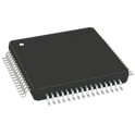
R7FA6E10F2CFM#AA0
ARM® Cortex®-M33 RA6E1 Microcontroller IC 32-Bit 200MHz 1MB (1M x 8) FLASH 64-LFQFP (10x10) ## Engineering Specification ## General Description The **R7FA6E10F2CFM#AA0** is a Renesas Electronics **RA6E1 series microcontroller** designed for embedded control, industrial electronics, IoT edge devices, automation systems, and general-purpose connected applications. It is built around an **Arm Cortex-M33 processor with TrustZone support**, providing high performance, secure execution capability, and flexible integration for modern embedded designs. ## Device Identification Manufacturer Part Number: **R7FA6E10F2CFM#AA0** Manufacturer: **Renesas Electronics** Product Family: **RA Family** Series: **RA6 Series** Group: **RA6E1 Group** Device Category: **Integrated Circuit** Device Type: **Microcontroller Unit** ## Core and Processing The device uses an **Arm Cortex-M33 core** and is intended for high-performance embedded processing. It supports secure application development through TrustZone technology and is suitable for systems requiring reliable control, fast response, and efficient software execution. ## Memory Configuration The microcontroller includes program flash memory, data flash memory, and SRAM resources suitable for embedded firmware, application code, configuration storage, and runtime processing requirements. ## Package and Mechanical Description The component is supplied in an **LQFP surface-mount package**, making it suitable for compact printed circuit board layouts and standard automated assembly processes. ## Electrical and Operating Description The device is designed for low-voltage embedded systems and supports operation across an industrial temperature range. It is suitable for products requiring stable performance in controlled, commercial, or industrial operating environments. ## Communication and Interface Support The device supports common embedded communication interfaces such as USB, UART, SPI, I²C, QSPI, and CAN, allowing integration with sensors, displays, external memory, communication modules, and other peripheral devices. ## Analog and Control Features The microcontroller includes analog conversion capability, timer functions, PWM support, watchdog protection, reset monitoring, and low-voltage detection features. These functions make it suitable for control systems, monitoring equipment, and mixed-signal embedded applications. ## Security and Debug Features The device supports embedded security functions including TrustZone, unique device identification, and true random number generation. Debug and development access is supported through standard JTAG and SWD interfaces. ## Application Suitability This device is suitable for embedded controllers, IoT devices, industrial automation, metering equipment, appliance control, USB-connected products, sensor-based systems, and general electronic control applications requiring a compact and secure microcontroller solution. ## Hashtags #commonpartslibrary #integratedcircuit #microcontroller #renesas #renesaselectronics #ra6e1 #ra6series #armcortexm33 #embeddedsystems #electronicscomponents #semiconductor #mcu #iotdevices #industrialautomation #pcbdesign #electronicparts #componentlibrary #engineeringparts #hardwaredesign #electronicsengineering
0 Uses0 Stars1085
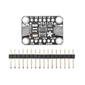
ADS1115 series 16 Bit 860 Samples per Second Analog to Digital Converter (ADC) Evaluation Board Adafruit 1085 ADS1115 Adafruit 4-Channel ADC Breakout based on Texas Instruments ADS1115 (16-bit) or ADS1015 (12-bit) analog-to-digital converter, featuring I2C communication, four single-ended inputs or two differential inputs, programmable gain amplifier (PGA) up to x16, internal voltage reference, programmable comparator, and selectable I2C addresses (0x48–0x4B). Operates from 2.0V to 5.5V and supports interfacing analog sensors with 3.3V and 5V microcontrollers such as Arduino, ESP32, STM32, RP2040, and Raspberry Pi. Search Keywords: Adafruit 4-Channel ADC Breakout, ADS1115 Breakout, ADS1015 Breakout, Adafruit ADS1115, Adafruit ADS1015, I2C ADC Module, 16-bit ADC, 12-bit ADC, 4-channel ADC, differential ADC, programmable gain amplifier, PGA ADC, analog sensor interface, TI ADS1115, TI ADS1015, Raspberry Pi ADC, Arduino ADC module, ESP32 ADC expansion Hashtags: #Adafruit #ADS1115 #ADS1015 #ADCModule #I2CADC #16BitADC #12BitADC #AnalogToDigitalConverter #SensorInterface #DifferentialADC #PGA #Arduino #ESP32 #STM32 #RP2040 #RaspberryPi #DataAcquisition #EmbeddedSystems #AdafruitBreakout
19 Uses0 StarsADPD7000BCBZR7
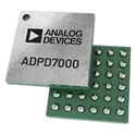
4 Channel AFE 12 Bit 36-WLCSP (2.8x2.56) The ADPD7000 is a highly integrated analog front end (AFE) designed for measuring various vital signals. The optical channel is designed as an optical transceiver, stimulating up to eight light emitting diodes (LEDs) and measuring the return signal on up to four separate current inputs. The signal chain rejects signal offsets and corruption from asynchronous modulated interference, typically from ambient light, eliminating the need for optical filters or externally controlled DC cancellation circuitry. The electrocardiography (ECG) signal acquisition is designed to support low noise, diagnostic level measurement in the presence of a variety of interferers. The ECG signal chain has a number of complementary features supporting ECG measurement, such as driven reference for common-mode rejection and lead off detection to identify a fallen electrode. The body impedance analysis (BIA) signal chain is designed for body impedance measurement with a configurable excitation path and measurement path. A 12-bit digital-to-analog converter (DAC) is used in the excitation path to generate the sinusoid wave and high precision measurement, with configurable filters used to measure the body response of the stimulus. The electrodermal activity (EDA) signal chain is designed for electrodermal activity. By multiplexing BIA and ECG peripheral circuits, the ADPD7000 supports high precision AC and DC measurement with 1 nS resolution. The data output and functional configuration use a serial port interface (SPI) on the ADPD7000. The control circuitry includes flexible LED signaling and synchronous detection, digital filters, digital wave generators, and configurable filters. The ADPD7000 is available in a 2.795 mm × 2.560 mm, 0.40 mm pitch, 36-ball WLCSP. ► Multimodal analog front end ► Optical channel ► 4 input channels with multiple operation modes for various sensor measurements ► 4-channel processing with simultaneous sampling ► 12 programmable time slots for synchronized sensor measurements ► Flexible input multiplexing to support single-ended sensor measurements ► 8 LED drivers, 2 of which can be driven simultaneously ► Flexible sampling rate from 0.004 Hz to 9 kHz using internal oscillators ► AC ambient light rejection: 78 dB up to 100 Hz ► 400 mA total LED peak drive current ► Individual ambient cancellation DAC at TIA input with 9-bit control up to 300 μA ► Individual LED DC cancellation DAC at TIA input with 7-bit control up to 190 μA ► ECG channel ► <1 µV RMS RTI noise at diagnosis bandwidth ► High input impedance 20 GΩ ► Accepts up to ±1.2 V of DC differential input range ► CMRR: 115 dB ► Flexible 4 electrode configurations to support various applications ► Both AC lead off detection and DC lead off detection ► Support always on, low power, lead on detection ► BIA channel ► Low power, high accuracy excitation path ► Configurable excitation frequency up to 250 kHz ► Sine wave excitation with a 12-bit DAC ► High accuracy with large imbalance contact impedance ≤20 kΩ ► Configurable receive filters with low noise design ► Complex impedance measurement engine ► Integrated current-limit resistors ► EDA channel ► Support both voltage excitation and current excitation ► 10 kΩ to100 MΩ measurement range with 1 nS resolution ► DFT and decimation for high accuracy measurement result ► SPI communications supported ► 704-byte FIFO
4 Uses0 StarsMAX2871ETJ+
Maxim Integrated PLL Frequency Synthesizer Single 23.5MHz to 6000MHz 32-Pin TQFN EP QFN-32 Maxim None MAX2871ETJ+ Unavailable Maxim Integrated MAX2871 ultra-wideband fractional-N / integer-N PLL frequency synthesizer with integrated VCOs, capable of generating RF frequencies from 23.5MHz to 6.0GHz. Features programmable output dividers (1/2/4/8/16/32/64/128), dual differential RF outputs with programmable output power from -1dBm to +8dBm, low phase noise performance, phase frequency detector up to 140MHz, reference frequency up to 210MHz, fast lock and cycle-slip reduction, automatic/manual VCO selection, on-chip temperature sensor with 7-bit ADC, 4-wire SPI-compatible serial interface, and operation from -40°C to +85°C. Suitable for wireless infrastructure, clock generation, microwave radios, RF signal generation, and test & measurement equipment. MAX2871 Search Keywords: MAX2871, Maxim MAX2871, Analog Devices MAX2871, PLL synthesizer, RF synthesizer, fractional N synthesizer, integer N synthesizer, 6GHz frequency synthesizer, RF signal generator IC, integrated VCO synthesizer, microwave synthesizer, SPI frequency synthesizer, dual output PLL, clock generation IC, wireless infrastructure synthesizer Hashtags: #MAX2871 #MaximIntegrated #AnalogDevices #PLLSynthesizer #FrequencySynthesizer #RFSynthesizer #FractionalNPLL #IntegerNPLL #IntegratedVCO #RFSignalGenerator #MicrowaveRadio #ClockGeneration #WirelessInfrastructure #SPIInterface #TestAndMeasurement #RFDesign #RFIC #PhaseLockedLoop
2 Uses0 StarsADC09SJ1300AAVT
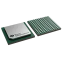
Analog to Digital Converters - ADC Single-channel, 9-bit, 1.3-GSPS analog-to-digital converter (ADC) with JESD204C interface 144-FCBGA -40 to 85 ADC09xJ1300 is a family of quad, dual and single channel, 9-bit, 1.3GSPS analog-to-digital converters (ADC). Low power consumption, high sampling rate and 9-bit resolution makes the ADC09xJ1300 ideally suited for suited for a variety of multi-channel communications and test systems. Full-power input bandwidth (-3dB) of 6GHz enables direct RF sampling of L-band and S-band. A number of clocking features are included to relax system hardware requirements, such as an internal phase-locked loop (PLL) with integrated voltagecontrolled oscillator (VCO) to generate the sampling clock. Four clock outputs are provided to clock the logic and SerDes of the FPGA or ASIC. A timestamp input and output is provided for pulsed systems. JESD204C serialized interface decreases system size by reducing the amount of printed circuit board (PCB) routing. Interface modes support from 2 to 8 lanes (dual and quad channel devices) or 1 to 4 lanes (for the single channel device), with SerDes baud-rates up to 17.16Gbps, to allow the optimal configuration for each application. Features • ADC Core: – Resolution: 9 Bit – Maximum sampling rate: 1.3GSPS – Non-interleaved architecture – Internal dither reduces high-order harmonics • Performance specifications (–1dBFS): – SNR (100 MHz): 53.5dBFS – ENOB (100 MHz): 8.5 Bits – SFDR (100 MHz): 64dBc – Noise floor (–20dBFS): –143dBFS • Full-scale input voltage: 80 mVPP-DIFF • Full-power input bandwidth: 6GHz • JESD204C Serial data interface: – Support for 2 to 8 (Quad/Dual channel) or 1 to 4 (Single channel) total SerDes lanes – Maximum baud-rate: 17.16Gbps – 64B/66B and 8B/10B encoding modes – Subclass-1 support for deterministic latency – Compatible with JESD204B receivers • Optional internal sampling clock generation – Internal PLL and VCO (7.2–8.2GHz) • SYSREF Windowing eases synchronization • Four clock outputs simplify system clocking – Reference clocks for FPGA or adjacent ADC – Reference clock for SerDes transceivers • Timestamp input and output for pulsed systems • Power consumption (1GSPS): – Quad Channel: 450mW / channel – Dual channel: 625mW / channel – Single channel: 940mW • Power supplies: 1.1V, 1.9V #CommonPartsLibrary #IntegratedCircuit #ADC #HighSpeedADC #RFADC #JESD204C #13GSPS #9bitADC #DirectRFSampling #TexasInstruments #MixedSignal #DataAcquisition #JESD204
0 Uses0 Stars