Transistors
A transistor is a type of electronic device that controls the flow of electricity or current through a circuit. It acts as a switch or gate, allowing current to pass through or blocking it, depending on the input signal applied to the transistor. Transistors are widely used in a variety of electronic devices and systems, including computers, televisions, radios, and smartphones. They are also used in a range of industrial and medical applications, such as power supply systems and medical equipment. Flux.ai is home to the world's largest community-driven public library of transistors, with footprints, symbols, datasheets, and simulation models available for a wide range of devices. The library is constantly being updated and expanded by a community of engineers and enthusiasts, making it an invaluable resource for anyone working with transistors. Whether you're a student, hobbyist, or professional engineer, you'll find everything you need to know about transistors at Flux.ai.
WMS08N06TS
Transistor: N-MOSFET; unipolar; 60V; 8A; Idm: 32A; 3.1W; SOP8 N-Channel MOSFET for power switching applications, featuring a 60V drain-source voltage (VDS), 80A continuous drain current (ID), and low RDS(on) for efficient conduction. It is housed in a PDFN 5×6 package and supports logic-level gate drive with a ±20 V gate-source voltage (VGS) rating. #NChannelMOSFET #PowerMOSFET #60V #80A #PDFN5x6 #LogicLevel #PowerSwitching
9 Uses0 Stars2N4416
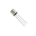
N-Channel Junction Field-Effect Transistor (JFET) – N-channel JFET optimized for high-frequency amplifiers, RF mixers, oscillators, analog switches, and low-noise signal amplification. Features a 30 V gate-to-source breakdown voltage (V(BR)GSS), 5 mA minimum drain current (IDSS) at VDS = 15 V, 3 V maximum gate-source cutoff voltage (VGS(off)), and 4 pF maximum input capacitance (Ciss) at VDS = 15 V for excellent high-frequency performance. Rated for 300 mW power dissipation, offers low noise and low distortion, and is specified for operation over a −50°C to +150°C junction temperature range. Housed in a 4-lead TO-206AF (TO-72 metal can) through-hole package. This part is obsolete and no longer manufactured. #Vishay #Siliconix #2N4416 #JFET #NChannelJFET #RFAmplifier #LowNoiseAmplifier #AnalogSwitch #Oscillator #Mixer #ThroughHole #TO72 #EmbeddedSystems
0 Uses0 StarsULN2003AIDR
Bipolar (BJT) Transistor Array Surface Mount 16-SOIC Darlington Transistor Array IC – High-voltage, high-current driver array containing seven NPN Darlington pairs with open-collector outputs. The ULN2003AIDR supports output voltage up to 50 V and collector current up to 500 mA per channel, with input-compatible logic levels and a 16-pin SOIC package. #DarlingtonArray #TransistorDriver #HighVoltageDriver #HighCurrentDriver #ULN2003A #TexasInstruments
41 Uses0 StarsSFH615A-3
Optocouplers - Phototransistor Output SFH615A-3 DIP-4_L4.6-W6.5-P2.54-LS7.6-BL SFH655A is a single-channel optocoupler with a GaAs infrared LED input and silicon photodarlington output, providing over 600% current transfer ratio and 5.3 kVrms isolation in a 4-pin through-hole DIP package. Keywords/Tags: SFH655, photodarlington optocoupler, 5300Vrms isolation, 4-pin DIP, transistor output optoisolator
5 Uses0 StarsTLP281(GB-TP,F)
Optoisolator Transistor Output 2500Vrms 1 Channel 4-SOP Photocoupler, a single-channel optically isolated device designed for signal transmission between electrically separated circuits. The TLP281(GB-TP,F) features a phototransistor output, AC input LED, isolation voltage rating of 3,750 Vrms, collector-emitter voltage of 80 V, and a compact 4-pin SO4 package. #Photocoupler #Optocoupler #PhototransistorOutput #ToshibaSemiconductor #TLP281 #PCBComponent #SignalIsolation #commonpartslibrary #isolator #optoisolator #transistor
22 Uses0 StarsAOD403
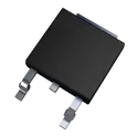
P-Channel 30V 15A (Ta), 70A (Tc) 2.5W (Ta), 90W (Tc) Surface Mount TO-252 (DPAK) P-channel enhancement-mode MOSFET designed for power switching applications, featuring a −30 V drain-source voltage, −70 A continuous drain current (at V<sub>GS</sub> = −20 V, T<sub>C</sub> = 25°C), and a maximum R<sub>DS(on)</sub> of 6.2 mΩ at V<sub>GS</sub> = −20 V (8 mΩ max at −10 V). The device uses advanced trench technology and is specified with ±25 V gate-source voltage, 100% UIS testing, and 100% gate resistance (R<sub>g</sub>) testing. #Commonpartslibrary #Transistor #P-Channel #MOSFET #PowerMOSFET #30V #HighCurrent #LowRDSon
21 Uses0 StarsKRC119S
Description: KRC119S is a KEC NPN digital transistor with built-in bias resistors, 50 V / 100 mA rating, R1 4.7 kΩ and R2 10 kΩ, supplied in a SOT-23 package for switching, interface, and driver circuits. Keywords: KRC119S, NPN digital transistor, bias resistor transistor, SOT-23, switching driver
0 Uses0 StarsIRFB4110PBF
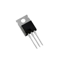
N-Channel 100V 120A (Tc) 370W (Tc) Through Hole TO-220AB Power MOSFET, N-channel enhancement-mode transistor designed for high-current switching applications. Features a 100 V drain-source voltage rating, 180 A continuous drain current, 3.7 mΩ maximum drain-source on-resistance, and TO-220AB package. #PowerMOSFET #NMOSFET #Infineon #IRFB4110PBF #TO220AB #commonpartslibrary #transistor #tht
274 Uses0 Stars