Timers and RTCs
Timers and Real-Time Clocks (RTCs) are electronic devices that are used to measure time or keep track of the current time. They can be found in a wide range of applications, including computers, phones, and appliances. Timers are used to trigger an action after a specific period of time has elapsed. They can be used to control the duration of an event, or to schedule tasks to be performed at a later time. RTCs, on the other hand, are used to maintain accurate time even when the device is powered off. They are often used in devices that need to keep track of the current time and date, such as alarm clocks and smart thermostats. If you're looking for high-quality timers and RTCs for your electronic projects, you should check out Flux.ai. They have the world's largest community-driven public library of timers and RTCs, with footprints, symbols, datasheets, and simulation models. This makes it easy for you to find the components you need for your project, and ensures that you have access to accurate and up-to-date information about each component. Whether you're a professional engineer or a hobbyist, Flux.ai has the resources you need to get your project off the ground.
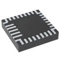
BQ25792RQMR
Charger IC Lithium Ion/Polymer 29-VQFN-HR (4x4) The BQ25792 is a switch-mode synchronous buck-boost charger with full power-path management. It can automatically regulate power flow between the input source, system load, and battery. It supports a wide input range and is designed for USB Type-C™ / USB Power Delivery (USB-PD) systems, enabling both charging and OTG (power output from battery) operation. ⭐ Key Features ⚡ High-performance charging Up to 5 A charge current Supports 1S to 4S battery packs High efficiency (up to ~96% under typical conditions) Programmable switching frequency: 750 kHz or 1.5 MHz 🔋 Wide input support Input voltage range: 3.6 V to 24 V Absolute max rating up to 30 V Supports USB adapters and barrel jack sources Detects USB charging standards (BC1.2, DCP, CDP, HVDCP, etc.) 🔄 Buck-boost power conversion Seamless buck, boost, and buck-boost operation Maintains stable system voltage even when battery is low or input varies 🔌 USB-PD / OTG support USB Power Delivery (PD 3.0 compatible) Supports OTG output (battery powers USB port) OTG voltage range: 2.8 V to 22 V 🧠 Intelligent power management NVDC power path management (system can run without battery) Dual-input power mux controller (select between two power sources) Battery supplement mode (prevents input overload) 📊 Monitoring & control Integrated 16-bit ADC for voltage, current, temperature monitoring Fully I²C configurable Autonomous or host-controlled operation 🛡️ Protection & safety Input and battery over-voltage/over-current protection Thermal regulation and shutdown Charging safety timer MOSFET protection (internal switching FETs included) 📦 Package 29-pin VQFN (4 mm × 4 mm) package Industrial temperature range: -40°C to 85°C #CommonPartsLibrary #IntegratedCircuit #PowerManagement #Battery-charger
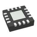
16 Uses0 StarsBQ25302RTER
Charger IC Lithium Ion/Polymer 16-WQFN (3x3) The BQ25302RTER is a highly integrated single-cell lithium-ion and lithium-polymer battery charger and power-path management IC developed by Texas Instruments. The device is optimized for compact portable and wearable applications requiring efficient battery charging from USB or low-voltage DC power sources. It integrates a switching charger, power-path management, system voltage regulation, battery FET, and protection features into a compact package suitable for space-constrained designs. The device supports programmable charging current and voltage regulation while maintaining high power conversion efficiency through its switching charger architecture. Integrated power-path management allows the system load to operate simultaneously while charging the battery, improving system reliability and startup behavior when the battery is deeply discharged or absent. The BQ25302RTER includes input current limiting, thermal regulation, battery temperature monitoring support, and multiple safety timers to ensure safe charging operation. The charger automatically manages preconditioning, fast charging, charge termination, and recharge cycles for lithium-based battery chemistries. The device also supports USB-compliant input operation and includes configurable features through an I2C-compatible interface. Its compact WQFN package and high integration level reduce external component count and PCB area, making it suitable for wearable electronics, portable medical devices, IoT products, handheld instruments, wireless accessories, and battery-powered embedded systems. Electrical Characteristics Input operating voltage supports standard USB and low-voltage DC input sources suitable for portable electronics applications. Supports single-cell lithium-ion and lithium-polymer battery charging with programmable charge voltage regulation. Integrated high-efficiency switching charger architecture minimizes power dissipation and improves thermal performance compared to linear chargers. Programmable fast-charge current supports flexible battery capacity scaling and application-specific charging requirements. Integrated power-path management allows simultaneous battery charging and system power delivery. Includes programmable input current limiting to support USB current compliance and adapter protection. Automatic charge cycle management includes precharge, fast charge, termination, and recharge operation. Supports battery temperature qualification using external thermistor monitoring. Integrated thermal regulation dynamically reduces charge current during high-temperature operating conditions. Low quiescent current operation improves standby battery life in portable products. Protection Features Integrated overvoltage protection for input power safety. Battery overcurrent and short-circuit protection enhance system reliability. Thermal shutdown circuitry protects the device during excessive junction temperature conditions. Safety timers monitor charging duration and prevent abnormal charging operation. Input current limiting protects USB ports and weak power adapters from overload conditions. Undervoltage lockout prevents improper operation during insufficient input supply conditions. Interface and Control I2C-compatible serial interface enables configuration and monitoring of charger parameters. Status reporting supports system-level battery and charging management. Programmable charging parameters allow firmware-controlled optimization for different battery chemistries and capacities. Interrupt and status functions support embedded power management architectures. Package Information Supplied in a compact WQFN package optimized for portable and space-constrained PCB layouts. Package design supports efficient thermal dissipation and automated surface-mount assembly processes. RoHS-compliant and suitable for modern lead-free manufacturing requirements. Typical Applications Wearable electronics Wireless earbuds and audio accessories Portable medical devices IoT and embedded battery-powered systems Handheld consumer electronics Portable instrumentation Rechargeable sensor modules Compact USB-powered battery charging systems #CommonPartsLibrary #IntegratedCircuit #PowerManagement #battery charger
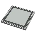
4 Uses0 StarsDSPIC33CK128MP205-I/M4
dsPIC dsPIC™ 33CK, Functional Safety (FuSa) Microcontroller IC 16-Bit 100MHz 128KB (128K x 8) FLASH 48-UQFN (6x6) 28/36/48/64/80-Pin Digital Signal Controllers with High-Resolution PWM and CAN Flexible Data (CAN FD) perating Conditions • 3.0V to 3.6V, -40°C to +125°C, DC to 100 MIPS • 3.0V to 3.6V, -40°C to +150°C, DC to 70 MIPS Core: 16-Bit dsPIC33CK CPU • 32-256 Kbytes of Program Flash with ECC and 8-24K RAM • Fast 6-Cycle Divide • LiveUpdate • Code Efficient (C and Assembly) Architecture • 40-Bit Wide Accumulators • Single-Cycle (MAC/MPY) with Dual Data Fetch • Single-Cycle, Mixed-Sign MUL Plus Hardware Divide • 32-Bit Multiply Support • Four Sets of Interrupt Context Saving Registers which Include Accumulator and STATUS for Fast Interrupt Handling • Zero Overhead Looping • RAM Memory Built-In Self-Test (MBIST) Clock Management • Internal Oscillator • Programmable PLLs and Oscillator Clock Sources • Reference Clock Output • Fail-Safe Clock Monitor (FSCM) • Fast Wake-up and Start-up • Backup Internal Oscillator Power Management • Low-Power Management Modes (Sleep, Idle, Doze) • Integrated Power-on Reset and Brown-out Reset High-Speed PWM • Eight PWM Pairs • Up to 250 ps PWM Resolution • Dead Time for Rising and Falling Edges • Dead-Time Compensation • Clock Chopping for High-Frequency Operation • PWM Support for: - DC/DC, AC/DC, inverters, PFC, lighting - BLDC, PMSM, ACIM, SRM motors • Fault and Current Limit Inputs • Flexible Trigger Configuration for ADC Triggering Timers/Output Compare/Input Capture • One General Purpose Timer • Peripheral Trigger Generator (PTG): - Up to 15 trigger sources to other peripheral modules - CPU independent state machine-based instruction sequencer • Nine MCCP/SCCP modules which Include Timer, Capture/Compare and PWM: - One MCCP - Eight SCCPs - 16 or 32-bit time base - 16 or 32-bit capture - 4-deep capture buffer • Fully Asynchronous Operation, Available in Sleep Modes
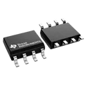
2 Uses0 StarsTLC555IDR
555 Type, Timer/Oscillator (Single) IC 2.1MHz 8-SOIC The TLC555IDR is a low-power CMOS timer device designed as a functional replacement for the standard bipolar 555 timer while providing significantly reduced supply current and improved operating efficiency. The device supports both astable and monostable operating modes and is commonly used for timing generation, pulse shaping, oscillation, PWM generation, delay circuits, and frequency generation applications. The CMOS architecture enables low power consumption, rail-to-rail output capability, and stable timing performance over a wide operating voltage range. The device is suitable for battery-powered systems, portable electronics, industrial controls, instrumentation, consumer products, and embedded electronic designs. The TLC555IDR is supplied in a compact SOIC surface-mount package intended for automated PCB assembly and space-constrained applications. Electrical Characteristics CMOS low-power timer architecture Functional equivalent to standard 555 timer devices Wide operating supply voltage range Low quiescent supply current High input impedance Rail-to-rail output swing capability Stable threshold and trigger levels Compatible with TTL and CMOS logic levels Capable of astable and monostable operation Adjustable duty cycle and frequency operation High output drive capability for direct interfacing Low noise and improved switching performance compared to bipolar 555 timers Functional Features Precision timing generation Oscillator and clock generation Pulse-width modulation support One-shot pulse generation Delay timer implementation Missing pulse detection Frequency divider implementation Sequential timing control LED flashing and tone generation PWM motor and power control applications Package Information Surface-mount SOIC package Standard tape-and-reel packaging format Compact footprint for automated assembly RoHS compliant device construction Environmental and Operating Conditions Industrial operating temperature range ESD protection handling required Suitable for commercial and industrial embedded systems Designed for low-power electronic applications Typical Applications Timer circuits Pulse generators Oscillators PWM controllers LED flashers Alarm and tone generators Frequency generators Power management timing Embedded control systems Portable battery-powered electronics #commonpartslibrary #integratedcircuit #timer #oscillator
61 Uses0 StarsTPS259814ARPWR
Electronic Fuse Regulator High-Side 10A 10-VQFN-HR (2x2) The TPS25981xx family of eFuses is a highly integrated circuit protection and power management solution in a small package. The devices provide multiple protection modes using very few external components and are a robust defense against overloads, short circuits, voltage surges and excessive inrush current. Output slew rate and inrush current can be adjusted using a single external capacitor. Loads are protected from input overvoltage conditions by cutting off the output if input exceeds an adjustable overvoltage threshold. The devices respond to output overload by actively limiting the current (during startup) or breaking the circuit (during steady-state). The overcurrent protection threshold as well as the transient overcurrent blanking timer are useradjustable. The current limit control pin also functions as an analog load current monitor. The devices are available in a 2-mm × 2-mm, 10- pin HotRod™ QFN package for improved thermal performance and reduced system footprint. The devices are characterized for operation over a junction temperature range of –40°C to +125°C. • Wide operating input voltage range: 2.7 V to 16 V – 20-V absolute maximum • Integrated FET with low on-resistance: RON = 6 mΩ (typ.) • Fast overvoltage protection – Adjustable overvoltage lockout (OVLO) with 1.2-μs (typ.) response time • Overcurrent protection with load current monitor output (ILM) – Circuit-breaker response – Adjustable threshold (ILIM) 1.5 A – 11 A • ±10% accuracy for ILIM > 5 A – Adjustable transient blanking timer (ITIMER) to allow peak currents up to 2 × ILIM – Output load current monitor accuracy: ±10% (IOUT ≥ 3 A) • Fast-trip response for short-circuit protection – 640-ns (typ.) response time – Adjustable (2 × ILIM) and fixed thresholds • Active high enable input with adjustable undervoltage lockout threshold (UVLO) • Active low enable input with adjustable undervoltage lockout threshold (OVLO) • Adjustable output slew rate control (dVdt) • Option to drive external FET for reverse current blocking in disabled/OFF state • Overtemperature protection • Quick Output Discharge • Digital outputs – Power Good (PG) and fault indication (FLT) • UL 2367 recognition (pending) • IEC 62368 CB certification (pending) • Small footprint: QFN 2-mm × 2-mm, 0.45-mm pitch #CommonPartsLibrary #IntegratedCircuit #PowerManagement
29 Uses0 Stars