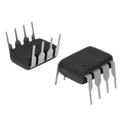
Timers and RTCs
Timers and Real-Time Clocks (RTCs) are electronic devices that are used to measure time or keep track of the current time. They can be found in a wide range of applications, including computers, phones, and appliances. Timers are used to trigger an action after a specific period of time has elapsed. They can be used to control the duration of an event, or to schedule tasks to be performed at a later time. RTCs, on the other hand, are used to maintain accurate time even when the device is powered off. They are often used in devices that need to keep track of the current time and date, such as alarm clocks and smart thermostats. If you're looking for high-quality timers and RTCs for your electronic projects, you should check out Flux.ai. They have the world's largest community-driven public library of timers and RTCs, with footprints, symbols, datasheets, and simulation models. This makes it easy for you to find the components you need for your project, and ensures that you have access to accurate and up-to-date information about each component. Whether you're a professional engineer or a hobbyist, Flux.ai has the resources you need to get your project off the ground.
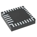
BQ25792RQMR
Charger IC Lithium Ion/Polymer 29-VQFN-HR (4x4) The BQ25792 is a fully integrated switch-mode buck-boost charger for 1-4 cell Li-ion batteries and Li-polymer batteries. The integration includes 4 switching MOSFETs (Q1, Q2, Q3, Q4), input and charging current sensing circuits, the battery FET (QBAT) and all the loop compensation of the buck-boost converter. It uses NVDC power path management, regulating the system slightly above the battery voltage without dropping below a configurable minimum system voltage. When system power exceeds the input source rating, battery supplement mode supports the system without overloading the input source. BQ25792 supports the full input and output (OTG) voltage ranges for USB Type-C™ and USB power delivery (USB-PD) applications. • High power density, high integration buck-boost charger for 1-4 cell batteries supporting any USB PD 3.0 profile – Integrates four switching MOSFETs, BATFET – Integrates input and charging current sensing • Highly efficient – 750-kHz or 1.5-MHz switching frequencies – 5-A charging current with 10-mA resolution • 96.5% efficient: 16-V battery at 3A from 20V • Supports a wide range of input sources – 3.6-V to 24-V wide input operating voltage range with 30-V absolute maximum rating – Maximum power tracking with input voltage dynamic power management (VINDPM) up to 22 V and input current dynamic power management (IINDPM) up to 3.3 A – Detects USB BC1.2, SDP, CDP, DCP, HVDCP and non-standard adapters • Dual-input power mux controller (optional) for source selection • Narrow voltage DC (NVDC) power path management • Powers USB port from battery (USB OTG) – 2.8-V to 22-V OTG output voltage with 10-mV resolution to support USB-PD PPS – OTG output current regulation up to 3.32 A with 40-mA resolution • Flexible autonomous and I2C mode for optimal system performance • Integrated 16-bit ADC for voltage, current, and temperature monitoring • Low battery quiescent current – 21 µA for battery only operation – 600 nA in Charger Shutdown Mode • High accuracy – +0.65% to -0.85% charge voltage regulation for 2S-4S batteries – ±5% charge current regulation – ±5% input current regulation • Safety – Thermal regulation and thermal shutdown – Input/battery OVP and OCP – Converter MOSFETs OCP – Charging safety timer • Package – 29-Pin 4 mm × 4 mm QFN #CommonPartsLibrary #IntegratedCircuit #PowerManagement #Battery-Charger
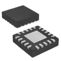
64 Uses0 StarsATTINY1616-MFR
ATTINY1616-MFR QFN-20_L3.0-W3.0-P0.40-TL-EP1.7 LCSC Part Number: C1338523 JLCPCB Part Class: Extended Part Manufactured by MICROCHIP(美国微芯) Microchip ATtiny1614/1616/1617 tinyAVR 1-series 8-bit microcontroller, AVR CPU running up to 20MHz, up to 16KB self-programmable Flash memory, 256B EEPROM and 2KB SRAM, 1.8V to 5.5V operating voltage range, single-pin UPDI programming and debug interface, power-on reset and brown-out detector, internal 16/20MHz oscillator, timers, watchdog, USART, SPI, I2C/TWI, 10-bit ADC, DAC, analog comparators, event system, configurable custom logic and peripheral touch controller, available in 14-pin, 20-pin and 24-pin packages depending on variant. Search Keywords: ATtiny1614, ATtiny1616, ATtiny1617, Microchip ATtiny1614, Microchip ATtiny1616, Microchip ATtiny1617, tinyAVR 1-series, AVR 8-bit microcontroller, ATtiny 16KB Flash, ATtiny UPDI, ATtiny1616 microcontroller, ATtiny1617 MCU, ATtiny1614 MCU, 20MHz AVR microcontroller, ATtiny I2C SPI USART, ATtiny1616 datasheet, ATtiny1614 datasheet, ATtiny1617 datasheet Hashtags: #ATtiny1614 #ATtiny1616 #ATtiny1617 #MicrochipATtiny #MicrochipMCU #tinyAVR #tinyAVR1Series #AVRMicrocontroller #8bitMicrocontroller #ATtinyMCU #UPDI #16KBFlashMCU #20MHzMCU #I2CMCU #SPIMCU #USARTMCU #ADCmicrocontroller #TouchControllerMCU
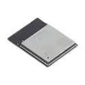
43 Uses0 StarsESP32-S3-MINI-1-N8
ESP32-S3-MINI-1-N8 is a compact, low-power Wi-Fi and Bluetooth module from Espressif Systems based on the ESP32-S3 SoC. It integrates a dual-core Xtensa LX7 processor, 8 MB flash memory, crystal oscillator, RF matching circuitry, and a PCB antenna in a small SMD package, making it ideal for IoT devices, smart home products, industrial automation, HMI applications, AIoT edge devices, and USB-connected embedded systems. Key Features Dual-core 32-bit Xtensa LX7 CPU Up to 240 MHz operating frequency Includes single-precision floating-point unit (FPU) for enhanced processing performance. Integrated Memory 8 MB Quad SPI Flash (N8 variant) 512 KB SRAM 384 KB ROM 16 KB RTC SRAM. Wireless Connectivity 2.4 GHz Wi-Fi 4 (802.11 b/g/n) Data rates up to 150 Mbps Bluetooth 5 LE with Bluetooth Mesh support Simultaneous Wi-Fi and Bluetooth operation through an integrated coexistence mechanism. Rich Peripheral Set Up to 39 GPIOs USB 2.0 OTG USB Serial/JTAG SPI, I²C, I²S, UART PWM, MCPWM SDIO Host ADC Touch sensing Temperature sensor TWAI® (CAN 2.0 compatible) Timers and watchdogs. Integrated Components On-board 40 MHz crystal oscillator PCB antenna RF matching network Compact certified module design. Operating Conditions Supply voltage: 3.0 V to 3.6 V Operating temperature: −40°C to +85°C. Compliance RoHS and REACH compliant RF-certified module for simplified product development. #RF_transceiver #Module #Esp32
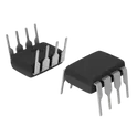
263 Uses0 StarsTLC555IP
555 Type, Timer/Oscillator (Single) IC 2.1MHz 8-PDIP The TLC555 is a CMOS monolithic timing circuit. The timer is fully compatible with CMOS, TTL, and MOS logic and operates at frequencies up to 2MHz. Because of a high input impedance, this device supports smaller timing capacitors than those supported by the NE555 or LM555. As a result, more accurate time delays and oscillations are possible. Power consumption is low across the full range of power-supply voltage. • Very low power consumption: – 1mW typical at VDD = 5V • Capable of operation in astable mode • CMOS output capable of swinging rail to rail • High output current capability – Sink: 100mA typical – Source: 10mA typical • Output fully compatible with CMOS, TTL, and MOS • Low supply current reduces spikes during output transitions • Single-supply operation from 2V to 15V • Functionally interchangeable with the NE555; has same pinout • ESD protection exceeds 1000V per ANSI/ESDA/ JEDEC JS-001 • Available in Q-temp automotive – High-reliability automotive applications – Configuration control and print support – Qualification to automotive standards #CommonPartsLibrary #IntegratedCircuit
95 Uses0 StarsTLC555CP
555 Type, Timer/Oscillator (Single) IC 2.1MHz 8-PDIP Like the NE555, the TLC555 has a trigger level equal to approximately one-third of the supply voltage and a threshold level equal to approximately two-thirds of the supply voltage. These levels can be altered by use of the control voltage terminal (CONT). When the trigger input (TRIG) falls below the trigger level, the flip-flop is set and the output goes high. If TRIG is above the trigger level and the threshold input (THRES) is above the threshold level, the flip-flop is reset and the output is low. The reset input (RESET) can override all other inputs and can be used to initiate a new timing cycle. If RESET is low, the flip-flop is reset and the output is low. Whenever the output is low, a low-impedance path is provided between the discharge terminal (DISCH) and GND. All unused inputs must be tied to an appropriate logic level to prevent false triggering. • Very low power consumption: – 1mW typical at VDD = 5V • Capable of operation in astable mode • CMOS output capable of swinging rail to rail • High output current capability – Sink: 100mA typical – Source: 10mA typical • Output fully compatible with CMOS, TTL, and MOS • Low supply current reduces spikes during output transitions • Single-supply operation from 2V to 15V • Functionally interchangeable with the NE555; has same pinout • ESD protection exceeds 1000V per ANSI/ESDA/ JEDEC JS-001 • Available in Q-temp automotive – High-reliability automotive applications – Configuration control and print support – Qualification to automotive standards #CommonPartsLibrary #IntegratedCircuit
235 Uses0 Stars