Sensors
A sensor is a device that detects and measures a physical property or phenomenon, such as temperature, pressure, or motion. Sensors are used in a wide range of applications, including industrial automation, environmental monitoring, healthcare, and transportation. Flux.ai is the world's largest community-driven public library of sensors, with footprints, symbols, datasheets, and simulation models. Our extensive collection of sensors covers a variety of use cases and industries, making it easy to find the perfect sensor for your application. Whether you need a temperature sensor for HVAC systems, a pressure sensor for automotive applications, or a motion sensor for security systems, Flux.ai has you covered. Our comprehensive library of sensors is constantly updated with the latest and most innovative technologies, ensuring that you have access to the best sensors available. So, if you need a sensor for your next project, be sure to check out Flux.ai and take advantage of our extensive collection and expert support.
RFFM6901
The RFFM6901 is a single-chip RF front-end module (FEM) designed for 868 MHz to 928 MHz ISM-band wireless communication applications. It integrates a high-power power amplifier (PA), low-noise amplifier (LNA), antenna diversity switch, and matching circuitry into a compact package, helping reduce external components, PCB space, and overall system cost. It is commonly used in smart energy systems, wireless metering, industrial monitoring, alarm systems, and other Sub-1 GHz wireless devices. Key Features Operating frequency range: 868 MHz to 928 MHz Integrated 1 W power amplifier Up to +30 dBm transmit output power Integrated low-noise amplifier with bypass mode Dual-port antenna diversity switch Separate 50 Ω transmit and receive interfaces Compact 32-pin LGA package (6 mm × 6 mm) Supply voltage range: 2.8 V to 4.2 V Typical LNA gain: 17 dB Low receiver noise figure: 1.5 dB Designed for portable and battery-powered wireless systems RoHS compliant Typical Applications Smart energy and smart metering Wireless alarm and security systems ISM-band communication devices Industrial wireless sensors Portable RF equipment IoT Sub-1 GHz wireless systems Search across more sources
2 Uses0 StarsPEC11J-9015F-S0024
Rotary Encoder Incremental 24 Quadrature (Incremental) User Selectable 10 mA @ 5 VDC,-10 C to +70 C The PEC11J-9015F-S0024 is a compact surface-mount incremental rotary encoder from the Bourns PEC11J series, designed for user interface applications requiring precise rotational input and long operational life. It features a quadrature output with 24 pulses per revolution and includes an integrated momentary push-button switch, making it suitable for menu navigation, volume control, tuning systems, and industrial control panels. Its rugged metal shaft construction and high durability make it reliable for both consumer and professional electronic equipment. Key Features Incremental rotary encoder with 2-bit quadrature output 24 pulses per revolution (24 PPR) resolution Integrated momentary push-button switch Surface-mount gull-wing terminals Compact 12 mm encoder body Durable metal shaft and bushing Long rotational life of up to 100,000 cycles No detents for smooth continuous rotation Supports up to 60 RPM operating speed Operating temperature range: -10 °C to +70 °C IP40 rated enclosure Flatted shaft design for secure knob attachment Suitable for: Audio equipment Lighting consoles Consumer appliances Communication devices Test and measurement equipment Component Category #Sensor #Encoder #Transducer #PEC11J
91 Uses0 StarsDS90UB953-Q1
2 MP MIPI® CSI-2 FPD-Link III serializer for 2MP/60fps cameras & radar The DS90UB953-Q1 is an automotive-grade high-speed serializer designed to convert parallel image sensor data into a high-speed serial stream for transmission over a single differential pair using FPD-Link III technology. It is intended for use in camera-based systems where compact cabling, high data integrity, and low latency are required. The device interfaces directly with image sensors through a MIPI CSI-2 input and transmits video, control, and GPIO data over a single coaxial or shielded twisted pair cable. Integrated clocking and control features allow synchronization with remote deserializers, enabling robust communication in electrically noisy environments typical of automotive and industrial applications. Functional Description The device receives image data from a connected sensor through a MIPI CSI-2 interface and serializes this data for transmission over a high-speed differential link. In addition to video data, bidirectional control communication is supported through an embedded control channel, allowing configuration and monitoring of remote devices using an I²C interface. The serializer incorporates programmable GPIO functionality that can be used for control signaling or sensor monitoring, with the ability to transport these signals across the link. Internal clock generation and phase-locked loop circuitry support multiple clocking modes, enabling flexible system design with either local or remote reference clocks. The device also includes pattern generation capabilities for system testing and validation. Electrical Characteristics The component operates from multiple power domains supporting core logic, I/O, and phase-locked loop functions. It is designed to provide stable high-speed signal transmission with controlled impedance outputs and low jitter characteristics. The differential serial output supports reliable long-distance communication over coaxial or twisted-pair media. Input interfaces are optimized for compatibility with standard MIPI CSI-2 signaling, ensuring seamless integration with modern image sensors. The control interface uses an open-drain I²C protocol for configuration and communication. Mechanical Characteristics The device is provided in a compact quad flat no-lead package suitable for high-density PCB designs. The package includes an exposed thermal pad that serves both as a heat dissipation path and a low-impedance electrical ground connection. The small footprint and low profile make it well suited for space-constrained applications such as camera modules and embedded vision systems. Environmental Characteristics The DS90UB953-Q1 is qualified for automotive applications and is designed to operate reliably over extended temperature ranges and under conditions of electrical noise, vibration, and mechanical stress. The device is compatible with standard surface-mount assembly processes, including lead-free reflow soldering. Materials and construction comply with relevant environmental and reliability standards for automotive-grade electronic components. Materials and Construction The package body is constructed from high-temperature thermally stable materials suitable for reflow soldering. Electrical contacts are formed from copper-based alloys with plated finishes to ensure long-term conductivity, corrosion resistance, and mechanical durability. The exposed pad is designed to interface directly with the PCB ground plane for improved thermal and electrical performance.
6 Uses0 StarsESP32-WROOM-32E (16MB)
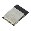
The ESP32-WROOM-32E (16MB) is a highly integrated Wi-Fi + Bluetooth + Bluetooth Low Energy (BLE) module developed by Espressif. It is based on the ESP32-D0WD-V3 chip and features a dual-core processor, rich peripherals, and large flash memory—making it ideal for IoT, embedded systems, and wireless applications. This module is part of the upgraded WROOM-32E series, offering improved RF performance, better stability, and enhanced reliability compared to earlier versions like the 32D. Key Features (16MB Variant) Processor & Memory Dual-core Xtensa® 32-bit LX6 CPU, up to 240 MHz 520 KB SRAM + 448 KB ROM 16 MB SPI Flash (large storage for firmware/data) Optional variants with PSRAM for memory-intensive tasks Connectivity 2.4 GHz Wi-Fi (802.11 b/g/n) Bluetooth v4.2 (BR/EDR + BLE) Integrated PCB antenna (no external antenna needed) Peripherals & Interfaces Up to 26–38 GPIOs (depending on usage) Supports: UART, SPI, I2C, I2S PWM (LED & motor control) ADC, DAC Capacitive touch sensors SD/SDIO/MMC, CAN (TWAI) Electrical & Physical Operating voltage: 3.0V – 3.6V Operating temperature: –40°C to +85°C (industrial range) Compact size: 18 × 25.5 × 3.1 mm Typical Applications Smart home devices (lighting, appliances) IoT sensors and gateways Industrial automation systems Wearables and smart gadgets Audio/voice processing (thanks to dual-core + large flash) #module #ESP32 #16MB
116 Uses0 StarsSSW-122-02-G-S
22 Position Receptacle Connector 0.100" (2.54mm) Through Hole Gold The SSW-122-02-G-S is a surface-mount, single-row socket strip designed for reliable board-to-board or component interconnection in electronic assemblies. It is part of a standardized connector series intended for applications requiring compact form factor, consistent electrical performance, and ease of automated placement. The component features a low-profile design suitable for dense PCB layouts and is commonly used in prototyping, embedded systems, and production-level electronics. Design and Construction The connector is manufactured with precision-aligned contacts housed in a high-temperature thermoplastic body, enabling compatibility with standard reflow soldering processes. The contact system is engineered to ensure stable mechanical retention and consistent electrical conductivity, supporting repeated mating cycles without significant degradation. The materials used provide durability, resistance to thermal stress, and compliance with common industry standards for electronic components. Electrical Characteristics The device is intended to provide reliable signal transmission with minimal contact resistance. It supports low to moderate current applications typical of signal-level interconnections. The contact plating is designed to reduce oxidation and maintain stable electrical performance over time. Mechanical Features The connector is configured as a single-row socket with a defined pitch spacing suitable for standard header interfaces. Its surface-mount termination allows for secure attachment to printed circuit boards while minimizing required board space. The structure supports proper alignment during assembly and ensures consistent engagement with corresponding mating connectors. Applications This component is widely used in applications such as microcontroller boards, communication modules, sensor interfaces, and general-purpose electronic systems. It is suitable for both development environments and final product integration where dependable and space-efficient connectivity is required. Compliance and Reliability The SSW-122-02-G-S is designed to meet common industry requirements for environmental and mechanical reliability. It is typically compliant with RoHS standards and suitable for use in a variety of operating conditions encountered in commercial and industrial electronics. #commonpartslibrary #connector #header
36 Uses0 StarsLM393N
Comparator Standard (General Purpose) Open-Collector, Rail-to-Rail 8-PDIP The LM393N is a dual independent voltage comparator designed for operation from a single power supply over a wide range of voltages. It can also operate from split power supplies, allowing flexible integration into analog and mixed-signal systems. Each comparator features high gain and low input offset voltage, enabling precise comparison between two input signals. The device is optimized for low power consumption and supports open-collector outputs, making it suitable for interfacing with a variety of logic families and external circuits. Its robust design allows reliable performance across a broad temperature range, making it appropriate for industrial, automotive, and consumer applications. Functional Overview The device contains two separate comparators sharing a common power supply. Each comparator compares the voltage at its inverting and non-inverting inputs and drives the output transistor accordingly. The open-collector output stage allows wired-OR configurations and easy level shifting using an external pull-up resistor. When the non-inverting input voltage exceeds the inverting input voltage, the output transistor turns off, allowing the output to be pulled high externally. When the inverting input is higher, the transistor conducts and pulls the output low. Electrical Characteristics The LM393N operates over a wide supply voltage range and exhibits low input bias current and low input offset voltage, contributing to stable and accurate performance. The input common-mode voltage range includes ground, enabling ground-referenced sensing. The output stage is capable of sinking current sufficient to drive loads such as LEDs, relays (with appropriate buffering), or logic inputs. The device is designed for low supply current, supporting energy-efficient designs. Input and Output Behavior Inputs are high impedance and suitable for direct connection to sensors, reference voltages, or signal conditioning networks. The output requires an external pull-up resistor to define the high logic level. This configuration allows flexibility in selecting output voltage levels independent of the supply voltage, within device limits. The open-collector structure also supports multiple outputs connected together for logical operations. Thermal and Environmental Conditions The device is specified for operation across a wide temperature range, ensuring stable functionality under varying environmental conditions. Proper thermal management and adherence to recommended operating conditions ensure long-term reliability. Packaging and Pin Configuration The LM393N is typically provided in a dual in-line package suitable for through-hole mounting. The pin configuration supports two independent comparator channels, each with inverting input, non-inverting input, and output, along with shared power supply and ground connections. Applications The LM393N is suitable for voltage level detection, threshold sensing, zero-crossing detection, oscillator circuits, pulse generation, and analog-to-digital interfacing. It is commonly used in power management systems, battery monitoring, signal conditioning, and embedded control systems. Design Considerations External components such as pull-up resistors, input filtering networks, and hysteresis feedback may be required depending on the application. Careful layout and noise considerations improve performance in high-sensitivity circuits. The open-collector output requires proper configuration to ensure correct logic levels and switching behavior. #commonpartslibrary #integratedcircuit #comparator
29 Uses0 StarsPAT9125EL-TKIT
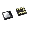
The PAT9125EL-TKIT from PixArt Imaging Inc. is a low-power optical tracking miniature chip designed for precise motion detection using laser-based optical navigation technology. It integrates both the optical sensor and VCSEL laser light source into a single compact package, enabling accurate tracking even on smooth or glossy surfaces. This device captures sequential surface images and processes them internally to determine movement direction, speed, and displacement (X/Y data), which can be accessed by a host controller via digital interfaces. It is particularly suited for space-constrained, battery-powered, and enclosed systems, eliminating the need for mechanical components like code wheels or special surface markings. Key Features Integrated optical sensor + VCSEL laser (850 nm) in a single package No external lens required, simplifying design Wide depth of field (DOF): 1–30 mm, even on reflective surfaces Programmable resolution up to ~1275 CPI Supports I²C (TKIT) interface (SPI variant available as TKMT) Motion detection interrupt output Built-in oscillator (no external clock needed) Low power consumption: Run: ~0.7 mA Sleep: down to 10 µA Power-down: ~5 µA Pre-calibrated laser (no calibration required) IEC/EN 60825-1 Class 1 eye-safe laser compliant Key Specifications Supply Voltage: VDD: 1.7–3.6 V VLD (laser): 2.7–3.6 V Max Tracking Speed: up to ~30 inches/sec Package: 8-pin LGA (3.5 × 3.2 × 1.0 mm) Interface: I²C (for TKIT variant)
5 Uses0 StarsADXL325BCPZ-RL7
Accelerometer X, Y, Z Axis ±5g 1.6kHz (X,Y), 550Hz (Z) 16-LFCSP-LQ (4x4) The ADXL325 is a small, low power, complete 3-axis accelerometer with signal conditioned voltage outputs. The product measures acceleration with a minimum full-scale range of ±5 g. It can measure the static acceleration of gravity in tilt-sensing applications, as well as dynamic acceleration, resulting from motion, shock, or vibration. The user selects the bandwidth of the accelerometer using the CX, CY, and CZ capacitors at the XOUT, YOUT, and ZOUT pins. Bandwidths can be selected to suit the application with a range of 0.5 Hz to 1600 Hz for X and Y axes and a range of 0.5 Hz to 550 Hz for the Z axis. The ADXL325 is available in a small, low profile, 4 mm × 4 mm × 1.45 mm, 16-lead, plastic lead frame chip scale package (LFCSP_LQ). 3-axis sensing Small, low profile package 4 mm × 4 mm × 1.45 mm LFCSP Low power: 350 μA typical Single-supply operation: 1.8 V to 3.6 V 10,000 g shock survival Excellent temperature stability Bandwidth adjustment with a single capacitor per axis RoHS/WEEE lead-free compliant #CommonPartsLibrary #Sensor #Transducer #Motion-Sensor #Accelerometer #ADXL325
6 Uses0 StarsADXL355BEZ
Accelerometer X, Y, Z Axis ±2g, 4g, 8g 1.5kHz 14-CLCC (6x6) General Description The ADXL355BEZ is a low noise, low drift, low power, three-axis MEMS accelerometer intended for high-precision sensing applications. It delivers high-resolution digital acceleration data with excellent long-term stability and minimal temperature-induced variation. The device integrates a complete sensing chain, including the MEMS sensor element, analog conditioning, analog-to-digital conversion, and digital filtering. Output data is provided through SPI or I²C interfaces, enabling straightforward integration into embedded and industrial systems. Key Features Three-axis acceleration sensing (X, Y, Z) Selectable full-scale ranges: ±2 g, ±4 g, ±8 g Low noise density (~25 µg/√Hz) Low offset and minimal temperature drift High-resolution 20-bit digital output Integrated digital filtering SPI and I²C communication interfaces Low power consumption (~200 µA typical) Wide supply voltage range (2.25 V to 3.6 V) Integrated temperature sensor Hermetically sealed package Applications Structural health monitoring Vibration measurement and analysis Tilt and inclination sensing Industrial condition monitoring Navigation and inertial systems Seismic detection Robotics and stabilization platforms Functional Description The ADXL355BEZ includes an integrated sensing and processing architecture composed of: Three-axis MEMS sensing element Analog front-end signal conditioning High-resolution ADC Digital filtering and decimation stages Temperature sensing element Digital communication interface (SPI/I²C) Configuration and control registers Electrical Characteristics (Typical) Supply voltage: 2.25 V to 3.6 V Supply current: ~200 µA Output data rate: up to 4 kHz Noise density: ~25 µg/√Hz Resolution: 20-bit Interface: SPI / I²C Mechanical and Package Information Package type: LGA (Land Grid Array) Approximate dimensions: 3 mm × 5 mm × 1 mm Hermetically sealed for improved environmental robustness Interface and Communication Supports SPI (4-wire) and I²C protocols Outputs 20-bit acceleration data per axis Data format: two’s complement Measurement Ranges ±2 g ±4 g ±8 g Environmental Specifications Operating temperature range: -40°C to +125°C Storage temperature range: -55°C to +150°C Power Management Supports measurement and standby modes Designed for low-power operation in continuous sensing applications Compliance and Reliability Industrial-grade device Designed for long-term stability RoHS compliant #commonpartslibrary #sensor #accelerometer
28 Uses0 Stars