Memory
A memory IC, or integrated circuit, is a type of electronic device that stores and retrieves data. It is used in a wide range of electronic devices, including computers, smartphones, and other electronic devices. Memory ICs come in a variety of types, including DRAM, SRAM, and Flash memory, and are used for different purposes depending on the device and application. One of the primary use cases for memory ICs is in computer systems, where they are used to store data and instructions that are accessed by the processor. Memory ICs are also used in a variety of other electronic devices, such as digital cameras, MP3 players, and mobile phones, to store data and enable various functions. Flux.ai has the world's largest community-driven public library of memory ICs, with a wide variety of footprints, symbols, datasheets, and simulation models available. This extensive library allows users to easily access and use memory ICs in their projects, making it an invaluable resource for engineers and developers.
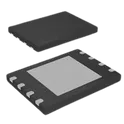
W25Q128JVPIQ
SPI Flash Memory with Dual/Quad SPI The W25Q128JV (128M-bit) Serial Flash memory provides a storage solution for systems with limited space, pins and power. The 25Q series offers flexibility and performance well beyond ordinary Serial Flash devices. They are ideal for code shadowing to RAM, executing code directly from Dual/Quad SPI (XIP) and storing voice, text and data. The device operates on a single 2.7V to 3.6V power supply with current consumption as low as 1µA for power-down. All devices are offered in space-saving packages. The W25Q128JV array is organized into 65,536 programmable pages of 256-bytes each. Up to 256 bytes can be programmed at a time. Pages can be erased in groups of 16 (4KB sector erase), groups of 128 (32KB block erase), groups of 256 (64KB block erase) or the entire chip (chip erase). The W25Q128JV has 4,096 erasable sectors and 256 erasable blocks respectively. The small 4KB sectors allow for greater flexibility in applications that require data and parameter storage. (See Figure 2.) The W25Q128JV supports the standard Serial Peripheral Interface (SPI), Dual/Quad I/O SPI: Serial Clock, Chip Select, Serial Data I/O0 (DI), I/O1 (DO), I/O2 and I/O3. SPI clock frequencies of W25Q128JV of up to 133MHz are supported allowing equivalent clock rates of 266MHz (133MHz x 2) for Dual I/O and 532MHz (133MHz x 4) for Quad I/O when using the Fast Read Dual/Quad I/O. These transfer rates can outperform standard Asynchronous 8 and 16-bit Parallel Flash memories. New Family of SpiFlash Memories – W25Q128JV: 128M-bit / 16M-byte – Standard SPI: CLK, /CS, DI, DO – Dual SPI: CLK, /CS, IO0, IO1 – Quad SPI: CLK, /CS, IO0, IO1, IO2, IO3 – Software & Hardware Reset(1) Highest Performance Serial Flash – 133MHz Single, Dual/Quad SPI clocks – 266/532MHz equivalent Dual/Quad SPI – 66MB/S continuous data transfer rate – Min. 100K Program-Erase cycles per sector – More than 20-year data retention Efficient “Continuous Read” – Continuous Read with 8/16/32/64-Byte Wrap – As few as 8 clocks to address memory – Allows true XIP (execute in place) operation Low Power, Wide Temperature Range – Single 2.7 to 3.6V supply – <1µA Power-down (typ.) – -40°C to +85°C operating range – -40°C to +105°C operating range Flexible Architecture with 4KB sectors – Uniform Sector/Block Erase (4K/32K/64K-Byte) – Program 1 to 256 byte per programmable page – Erase/Program Suspend & Resume Advanced Security Features – Software and Hardware Write-Protect – Power Supply Lock-Down – Special OTP protection – Top/Bottom, Complement array protection – Individual Block/Sector array protection – 64-Bit Unique ID for each device – Discoverable Parameters (SFDP) Register – 3X256-Bytes Security Registers with OTP locks – Volatile & Non-volatile Status Register Bits Space Efficient Packaging – 8-pin SOIC 208-mil – 16-pin SOIC 300-mil (additional /RESET pin) – 8-pad WSON 6x5-mm / 8x6-mm – 24-ball TFBGA 8x6-mm (6x4/5x5 ball array) – 24-ball WLCSP – Contact Winbond for KGD and other options #CommonPartsLibrary #IntegratedCircuit #Memory
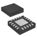
38 Uses0 StarsATTINY1616-MFR
ATTINY1616-MFR QFN-20_L3.0-W3.0-P0.40-TL-EP1.7 LCSC Part Number: C1338523 JLCPCB Part Class: Extended Part Manufactured by MICROCHIP(美国微芯) Microchip ATtiny1614/1616/1617 tinyAVR 1-series 8-bit microcontroller, AVR CPU running up to 20MHz, up to 16KB self-programmable Flash memory, 256B EEPROM and 2KB SRAM, 1.8V to 5.5V operating voltage range, single-pin UPDI programming and debug interface, power-on reset and brown-out detector, internal 16/20MHz oscillator, timers, watchdog, USART, SPI, I2C/TWI, 10-bit ADC, DAC, analog comparators, event system, configurable custom logic and peripheral touch controller, available in 14-pin, 20-pin and 24-pin packages depending on variant. Search Keywords: ATtiny1614, ATtiny1616, ATtiny1617, Microchip ATtiny1614, Microchip ATtiny1616, Microchip ATtiny1617, tinyAVR 1-series, AVR 8-bit microcontroller, ATtiny 16KB Flash, ATtiny UPDI, ATtiny1616 microcontroller, ATtiny1617 MCU, ATtiny1614 MCU, 20MHz AVR microcontroller, ATtiny I2C SPI USART, ATtiny1616 datasheet, ATtiny1614 datasheet, ATtiny1617 datasheet Hashtags: #ATtiny1614 #ATtiny1616 #ATtiny1617 #MicrochipATtiny #MicrochipMCU #tinyAVR #tinyAVR1Series #AVRMicrocontroller #8bitMicrocontroller #ATtinyMCU #UPDI #16KBFlashMCU #20MHzMCU #I2CMCU #SPIMCU #USARTMCU #ADCmicrocontroller #TouchControllerMCU
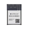
47 Uses0 StarsESP32-S3-WROOM-1-N8
ESP32-S3-WROOM-1-N8 is a high-performance Wi-Fi and Bluetooth Low Energy (BLE) module from Espressif Systems. It is built around the ESP32-S3 SoC, featuring a dual-core Xtensa LX7 processor, integrated 2.4 GHz Wi-Fi and Bluetooth 5 LE connectivity, 8 MB SPI flash memory, and a PCB antenna. The module is optimized for AIoT, edge computing, human-machine interfaces, smart devices, and industrial IoT applications. Key Features Dual-core Xtensa® LX7 CPU running up to 240 MHz for high-performance embedded applications. 8 MB onboard SPI Flash (N8 variant) for firmware and data storage. 2.4 GHz Wi-Fi (802.11 b/g/n) with data rates up to 150 Mbps. Bluetooth 5 LE support including: Long Range mode 2 Mbps PHY Bluetooth Mesh Extended Advertising AI acceleration support through ESP32-S3 vector instructions for machine learning and signal-processing workloads. USB 1.1 OTG and USB Serial/JTAG integrated, simplifying debugging and USB device applications. Up to 45 GPIOs with extensive peripheral support: SPI I²C I²S UART PWM ADC Touch Sensors TWAI® (CAN-compatible) Camera Interface LCD Interface SDIO Host MCPWM Integrated 40 MHz crystal oscillator, RF matching circuitry, and PCB antenna for reduced external component count. Operating voltage range: 3.0 V to 3.6 V. Compact surface-mount module suitable for space-constrained designs. Typical Applications Smart home and home automation devices HMI displays and touchscreen products Voice recognition and audio processing Edge AI and machine learning applications Industrial IoT gateways and sensors Video streaming and camera systems USB-connected embedded devices Smart agriculture and healthcare equipment N8 specifically indicates 8 MB Flash and no PSRAM, making it a good choice for applications requiring substantial program storage but not large external RAM. #RF-transceiver #Module #ESP32
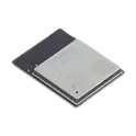
181 Uses0 StarsESP32-S3-MINI-1-N8
ESP32-S3-MINI-1-N8 is a compact, low-power Wi-Fi and Bluetooth module from Espressif Systems based on the ESP32-S3 SoC. It integrates a dual-core Xtensa LX7 processor, 8 MB flash memory, crystal oscillator, RF matching circuitry, and a PCB antenna in a small SMD package, making it ideal for IoT devices, smart home products, industrial automation, HMI applications, AIoT edge devices, and USB-connected embedded systems. Key Features Dual-core 32-bit Xtensa LX7 CPU Up to 240 MHz operating frequency Includes single-precision floating-point unit (FPU) for enhanced processing performance. Integrated Memory 8 MB Quad SPI Flash (N8 variant) 512 KB SRAM 384 KB ROM 16 KB RTC SRAM. Wireless Connectivity 2.4 GHz Wi-Fi 4 (802.11 b/g/n) Data rates up to 150 Mbps Bluetooth 5 LE with Bluetooth Mesh support Simultaneous Wi-Fi and Bluetooth operation through an integrated coexistence mechanism. Rich Peripheral Set Up to 39 GPIOs USB 2.0 OTG USB Serial/JTAG SPI, I²C, I²S, UART PWM, MCPWM SDIO Host ADC Touch sensing Temperature sensor TWAI® (CAN 2.0 compatible) Timers and watchdogs. Integrated Components On-board 40 MHz crystal oscillator PCB antenna RF matching network Compact certified module design. Operating Conditions Supply voltage: 3.0 V to 3.6 V Operating temperature: −40°C to +85°C. Compliance RoHS and REACH compliant RF-certified module for simplified product development. #RF_transceiver #Module #Esp32
327 Uses0 Stars