Memory
A memory IC, or integrated circuit, is a type of electronic device that stores and retrieves data. It is used in a wide range of electronic devices, including computers, smartphones, and other electronic devices. Memory ICs come in a variety of types, including DRAM, SRAM, and Flash memory, and are used for different purposes depending on the device and application. One of the primary use cases for memory ICs is in computer systems, where they are used to store data and instructions that are accessed by the processor. Memory ICs are also used in a variety of other electronic devices, such as digital cameras, MP3 players, and mobile phones, to store data and enable various functions. Flux.ai has the world's largest community-driven public library of memory ICs, with a wide variety of footprints, symbols, datasheets, and simulation models available. This extensive library allows users to easily access and use memory ICs in their projects, making it an invaluable resource for engineers and developers.
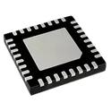
STM32L432KCU6
ST Microelectronics STM32L432KCU6 UFQFPN-32_L5.0-W5.0-P0.50-TL-EP3.5 LCSC Part Number: C1337280 JLCPCB Part Class: Extended Part Manufactured by ST(意法半导体) STMicroelectronics STM32L432KC ultra-low-power 32-bit ARM Cortex-M4 microcontroller with FPU running up to 80MHz, featuring 256KB Flash memory, 64KB SRAM, USB 2.0 Full-Speed device support, Quad-SPI interface, RTC with calendar and alarms, true random number generator (TRNG), DMA controller, CAN 2.0B, UART, LPUART, SPI, I2C, SAI audio interface, 12-bit 5MSPS ADC, dual 12-bit DACs, operational amplifier with PGA, comparators, capacitive sensing channels, advanced timers and ultra-low-power modes. Operates from 1.71V to 3.6V and is optimized for battery-powered, industrial, medical, IoT and portable embedded applications. Search Keywords: STM32L432KC, STM32L432KCU6, STM32L432KCU6TR, STM32L432, STM32L4 series, STM32 Cortex-M4 MCU, STM32 low power microcontroller, STM32 256KB Flash 64KB SRAM, STM32 USB FS MCU, STM32 CAN MCU, STM32 Quad SPI MCU, STM32L432 datasheet, STM32L432 development board, Nucleo-L432KC, ARM Cortex-M4 FPU Hashtags: #STM32L432KC #STM32L432KCU6 #STM32L432 #STM32L4 #STMicroelectronics #CortexM4 #ARMMicrocontroller #LowPowerMCU #EmbeddedSystems #USBFS #CANBus #QuadSPI #ADC12bit #DAC12bit #RTC #TRNG #IoTMCU #IndustrialMCU #MedicalElectronics #NucleoL432KC
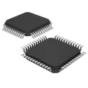
40 Uses0 StarsSTM32G0B1CBT6
ARM-MSeries LQFP-48(7x7) Microcontrollers (MCU/MPU/SOC) ROHS ST Microelectronics STM32G0B1CBT6 LQFP-48_L7.0-W7.0-P0.50-LS9.0-BL LCSC Part Number: C2847904 JLCPCB Part Class: Extended Part Manufactured by ST(意法半导体) STMicroelectronics STM32G0B1 series 32-bit Arm Cortex-M0+ microcontroller, up to 64MHz CPU frequency, 1.7V to 3.6V operating voltage, up to 512KB Flash memory and 144KB SRAM, USB 2.0 full-speed device/host support, USB Type-C Power Delivery controller, FDCAN, I2C, USART, SPI, HDMI CEC, 12-bit ADC, 12-bit DACs, timers, RTC, DMA, CRC unit, SWD debug interface, 96-bit unique ID, operating temperature options up to -40°C to +125°C, available in LQFP, UFQFPN, UFBGA and WLCSP packages. Search Keywords: STM32G0B1, STM32G0B1xB, STM32G0B1xC, STM32G0B1xE, STMicroelectronics STM32G0B1, STM32G0B1 MCU, STM32G0B1 microcontroller, Arm Cortex-M0+ microcontroller, STM32G0 64MHz MCU, STM32G0B1 USB Type-C PD, STM32G0B1 USB FS, STM32G0B1 FDCAN, STM32G0B1 512KB Flash, STM32G0B1 144KB SRAM, STM32G0B1 LQFP, STM32G0B1 UFQFPN, STM32G0B1 UFBGA, STM32G0B1 WLCSP, STM32G0B1 datasheet Hashtags: #STM32G0B1 #STM32G0B1xB #STM32G0B1xC #STM32G0B1xE #STMicroelectronics #STM32MCU #STM32G0 #ArmCortexM0Plus #32bitMicrocontroller #64MHzMCU #512KBFlashMCU #144KBSRAM #USBTypeCPD #USBFS #FDCAN #I2CMCU #SPIMCU #USARTMCU #ADCmicrocontroller #DACmicrocontroller #LQFP #UFQFPN #UFBGA #WLCSP
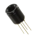
72 Uses0 StarsMLX90640ESF-BAB-000-TU
Thermal Image Sensor 32H x 24V TO-39 # MLX90640ESF-BAB-000-TU Engineering Specifications **General Description** The MLX90640ESF-BAB-000-TU is a contactless infrared thermal imaging sensor manufactured by Melexis. It incorporates a microbolometer array that detects infrared radiation emitted by objects and converts the captured thermal energy into temperature data, enabling the creation of thermal images without physical contact. The device is designed for compact and cost-effective thermal imaging applications, offering high thermal sensitivity and accurate temperature measurement capabilities. It integrates a digital signal-processing engine, calibration data memory, and a digital communication interface, allowing direct connection to microcontrollers, embedded systems, and industrial monitoring equipment. The sensor provides real-time thermal mapping across its field of view and is suitable for applications involving human presence detection, predictive maintenance, industrial automation, smart building systems, medical screening, consumer electronics, robotics, and thermal monitoring solutions. Its factory calibration ensures stable performance throughout its operating life while minimizing external calibration requirements. **Engineering Specifications** **Manufacturer:** Melexis **Manufacturer Part Number:** MLX90640ESF-BAB-000-TU **Component Type:** Infrared thermal imaging sensor **Sensor Technology:** Microbolometer thermal sensor array **Measurement Method:** Non-contact infrared temperature sensing **Output Type:** Digital thermal image data **Communication Interface:** I²C-compatible serial interface **Temperature Measurement Capability:** Object temperature monitoring and thermal imaging **Thermal Imaging Function:** Real-time thermal map generation **Integrated Processing:** On-chip signal processing and calibration management **Calibration:** Factory calibrated with stored calibration parameters **Power Supply Configuration:** Single-supply operation **Power Consumption:** Optimized for low-power embedded applications **Refresh Rate:** Programmable thermal frame refresh operation **Thermal Sensitivity:** High-sensitivity infrared detection **Field of View Variant:** Wide-angle thermal imaging configuration **Accuracy Characteristics:** High-precision temperature measurement with integrated compensation algorithms **Memory Features:** Internal EEPROM for calibration coefficients **Operating Mode:** Continuous and programmable thermal acquisition **Data Output Format:** Digital temperature and thermal pixel information **Environmental Stability:** Designed for reliable operation across varying ambient conditions **Electromagnetic Compatibility:** Suitable for embedded and industrial electronic systems **Package Type:** Surface-mount package with infrared-transparent window **Mounting Style:** Surface mount technology **Package Construction:** Reflow-solderable assembly **Lead Finish:** Lead-free finish **Environmental Compliance:** RoHS compliant and halogen-free **Reliability Features:** Factory-tested and production-calibrated thermal imaging device **Typical Applications** Thermal cameras Human presence detection systems Occupancy monitoring Industrial predictive maintenance Electrical equipment inspection Smart building automation HVAC monitoring systems Medical screening devices Consumer electronics Robotics and autonomous systems Fire detection and prevention systems Industrial process monitoring Energy management systems Automotive thermal sensing applications Security and surveillance equipment #MLX90640 #MLX90640ESF #Melexis #ThermalSensor #InfraredSensor #ThermalImaging #Microbolometer #TemperatureSensor #IndustrialAutomation #EmbeddedSystems #IoT #PredictiveMaintenance #SmartBuilding #ThermalCamera #ElectronicComponents #EngineeringSpecifications
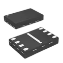
7 Uses0 StarsW25Q16JVUXIQ
SPI Flash Serial Flash Memory with Dual/Quad SPI The W25Q16JVUXIQ is a 16-Mbit (2-MByte) Serial NOR Flash memory device from Winbond. It is designed for embedded systems that require non-volatile code and data storage with minimal pin count, low power consumption, and high-speed access. The device supports standard SPI, Dual SPI, and Quad SPI interfaces, making it suitable for firmware storage, boot memory, IoT devices, microcontrollers, consumer electronics, and execute-in-place (XIP) applications. Key Features 16-Mbit (2-MByte) Flash Memory Capacity Operating Voltage: 2.7 V to 3.6 V Standard SPI, Dual SPI, and Quad SPI Interface Support Maximum SPI Clock Frequency: 133 MHz Equivalent Data Transfer Rates: 266 MHz (Dual SPI) 532 MHz (Quad SPI) Continuous Read and XIP (Execute-In-Place) Capability 4 KB Sector Erase, 32 KB Block Erase, 64 KB Block Erase, and Chip Erase 256-Byte Programmable Page Size Minimum 100,000 Program/Erase Cycles per Sector More Than 20 Years Data Retention Ultra-Low Power Consumption Typical power-down current below 1 µA 64-Bit Unique Serial Number Three 256-Byte Security Registers with OTP Protection JEDEC ID and SFDP Support Software and Hardware Write Protection Operating Temperature Options up to +85°C and +105°C Compact 8-Pad USON Package (2 mm × 3 mm) suitable for space-constrained designs #CommonPartsLibrary #IntegratedCircuit #Memory
167 Uses0 StarsW25Q128JVPIQ
SPI Flash Memory with Dual/Quad SPI The W25Q128JV (128M-bit) Serial Flash memory provides a storage solution for systems with limited space, pins and power. The 25Q series offers flexibility and performance well beyond ordinary Serial Flash devices. They are ideal for code shadowing to RAM, executing code directly from Dual/Quad SPI (XIP) and storing voice, text and data. The device operates on a single 2.7V to 3.6V power supply with current consumption as low as 1µA for power-down. All devices are offered in space-saving packages. The W25Q128JV array is organized into 65,536 programmable pages of 256-bytes each. Up to 256 bytes can be programmed at a time. Pages can be erased in groups of 16 (4KB sector erase), groups of 128 (32KB block erase), groups of 256 (64KB block erase) or the entire chip (chip erase). The W25Q128JV has 4,096 erasable sectors and 256 erasable blocks respectively. The small 4KB sectors allow for greater flexibility in applications that require data and parameter storage. (See Figure 2.) The W25Q128JV supports the standard Serial Peripheral Interface (SPI), Dual/Quad I/O SPI: Serial Clock, Chip Select, Serial Data I/O0 (DI), I/O1 (DO), I/O2 and I/O3. SPI clock frequencies of W25Q128JV of up to 133MHz are supported allowing equivalent clock rates of 266MHz (133MHz x 2) for Dual I/O and 532MHz (133MHz x 4) for Quad I/O when using the Fast Read Dual/Quad I/O. These transfer rates can outperform standard Asynchronous 8 and 16-bit Parallel Flash memories. New Family of SpiFlash Memories – W25Q128JV: 128M-bit / 16M-byte – Standard SPI: CLK, /CS, DI, DO – Dual SPI: CLK, /CS, IO0, IO1 – Quad SPI: CLK, /CS, IO0, IO1, IO2, IO3 – Software & Hardware Reset(1) Highest Performance Serial Flash – 133MHz Single, Dual/Quad SPI clocks – 266/532MHz equivalent Dual/Quad SPI – 66MB/S continuous data transfer rate – Min. 100K Program-Erase cycles per sector – More than 20-year data retention Efficient “Continuous Read” – Continuous Read with 8/16/32/64-Byte Wrap – As few as 8 clocks to address memory – Allows true XIP (execute in place) operation Low Power, Wide Temperature Range – Single 2.7 to 3.6V supply – <1µA Power-down (typ.) – -40°C to +85°C operating range – -40°C to +105°C operating range Flexible Architecture with 4KB sectors – Uniform Sector/Block Erase (4K/32K/64K-Byte) – Program 1 to 256 byte per programmable page – Erase/Program Suspend & Resume Advanced Security Features – Software and Hardware Write-Protect – Power Supply Lock-Down – Special OTP protection – Top/Bottom, Complement array protection – Individual Block/Sector array protection – 64-Bit Unique ID for each device – Discoverable Parameters (SFDP) Register – 3X256-Bytes Security Registers with OTP locks – Volatile & Non-volatile Status Register Bits Space Efficient Packaging – 8-pin SOIC 208-mil – 16-pin SOIC 300-mil (additional /RESET pin) – 8-pad WSON 6x5-mm / 8x6-mm – 24-ball TFBGA 8x6-mm (6x4/5x5 ball array) – 24-ball WLCSP – Contact Winbond for KGD and other options #CommonPartsLibrary #IntegratedCircuit #Memory
38 Uses0 Stars