Interface ICs
An interface IC is a type of integrated circuit that is designed to facilitate communication between two devices or systems. These devices are commonly used in electronic systems to enable the transfer of data and control signals between different components or subsystems. Some common use cases for interface ICs include connecting microcontrollers to peripherals such as sensors or displays, linking multiple processors together in a network, and enabling communication between devices using different communication protocols. Flux.ai has the world's largest community-driven public library of interface ICs, with footprints, symbols, datasheets, and simulation models. This library is a valuable resource for engineers and designers who need access to accurate and up-to-date information on these important components. Whether you are working on a new design project or simply looking to learn more about interface ICs, Flux.ai is an excellent resource to help you find the information you need.
ENW-89854A3KF
802.15.4, Bluetooth Bluetooth v5.0 Transceiver Module Integrated, Ceramic Patch Surface Mount General Description ENW-89854A3KF refers to a designated component, system, or configuration intended for engineering deployment within a defined operational environment. It is designed to meet performance, reliability, and integration requirements consistent with modern engineering standards. The specification outlines the functional expectations, structural considerations, and operational behavior necessary to ensure compatibility with associated systems and to support stable, efficient performance under expected conditions. Scope This specification defines the requirements and characteristics of ENW-89854A3KF, including its intended functionality, performance expectations, environmental tolerance, and integration considerations. It applies to design, development, testing, and implementation phases. Functional Requirements The system shall perform its intended function consistently within defined operational parameters. It shall support continuous operation where required and maintain stability under varying load conditions. The design shall ensure predictable behavior and allow for monitoring and control as necessary. Performance Characteristics The component shall operate efficiently within acceptable performance thresholds. It shall maintain responsiveness and reliability during standard and peak conditions. Performance degradation, if any, shall remain within acceptable engineering tolerances. Design Considerations The design shall prioritize durability, maintainability, and scalability. Materials and architecture shall be selected to ensure long-term operation with minimal failure risk. The system shall support ease of integration with existing infrastructure and allow for future modifications if required. Environmental Conditions The system shall operate within specified environmental ranges, including temperature, humidity, and exposure conditions relevant to its deployment context. Protective measures shall be incorporated where necessary to prevent damage or performance loss. Interface and Integration ENW-89854A3KF shall be compatible with associated systems and interfaces. Communication protocols, physical connections, and data exchange mechanisms shall align with standard engineering practices to ensure seamless integration. Safety and Compliance The design and operation shall adhere to applicable safety standards and regulatory requirements. The system shall include safeguards to prevent hazardous conditions and ensure safe handling and operation. Testing and Validation The system shall undergo verification and validation to confirm compliance with this specification. Testing shall include functional validation, performance assessment, and environmental resilience checks. Maintenance and Support The system shall be designed for ease of maintenance, including accessibility for inspection, repair, or replacement. Documentation and support provisions shall be available to ensure proper lifecycle management. #commonpartslibrary #integratedcircuit #transceiver #wireless #rf
0 Uses0 Stars0603L050YR
Polymeric PTC Resettable Fuse 6V 500 mA Ih Surface Mount 0603 (1608 Metric), Concave polyfuse 500mA 0603 The 0603L050YR is a surface-mount resettable fuse based on polymeric positive temperature coefficient technology, designed to provide overcurrent protection in compact electronic circuits. Under normal operating conditions, the device exhibits low resistance and allows current to pass with minimal power loss. When exposed to an overcurrent condition, the device transitions to a high-resistance state, effectively limiting the current and protecting downstream components. Once the fault condition is removed and power is cycled or the device cools, the fuse automatically resets to its original low-resistance state. This component is optimized for space-constrained applications requiring reliable, resettable protection, such as portable electronics, battery-powered systems, and low-voltage signal lines. Its small form factor enables integration into dense PCB layouts while maintaining compliance with industry safety standards for overcurrent protection. Package and Mounting: Surface-mount device in standard 0603 footprint, compatible with automated assembly processes including reflow soldering. Electrical Characteristics: The device is designed to maintain normal operation at a defined hold current level and transition to a protective state when the current exceeds its trip threshold. It operates within low-voltage circuits and provides fast response to fault conditions while minimizing nuisance tripping under typical load variations. Functional Behavior: The fuse operates by increasing resistance sharply in response to thermal energy generated by excess current. This behavior reduces current flow and limits fault energy. After removal of the overcurrent condition, the device gradually returns to its conductive state, enabling repeated use without replacement. Applications: Suitable for use in power lines, battery packs, USB interfaces, consumer electronics, and other low-voltage systems where resettable overcurrent protection is required. Compliance and Reliability: Designed to meet relevant safety and environmental standards for electronic components, ensuring stable performance across specified operating conditions and long-term reliability in field applications. #commonpartslibrary #fuse #Circuit-Protection #PTC #ptc #polymeric
202 Uses0 StarsTPD1E05U06DPYR
14V Clamp 2.5A (8/20µs) Ipp Tvs Diode Surface Mount 2-X1SON (1x.60) TVS diode USB VBUS 5V TVS diode USB VBUS 5V ESD protection General Description The TPD1E05U06DPYR is a single-channel transient voltage suppression device designed to protect sensitive electronic components from electrostatic discharge (ESD) and other transient voltage events. It is engineered for high-speed signal applications, offering low capacitance to preserve signal integrity while providing robust protection. The device is suitable for integration into compact and portable electronic systems where space, reliability, and performance are critical. Device Identification Part number: TPD1E05U06DPYR Device classification: ESD protection diode / transient voltage suppressor Manufacturer: Commonly associated with Texas Instruments Mounting type: Surface-mount Package style: Ultra-small leadless package (e.g., X2SON/DFN) Functional Description Protects circuits from high-voltage transients caused by ESD events Limits voltage spikes by clamping them to safe levels Maintains signal quality by minimizing added capacitance Operates transparently under normal signal conditions Provides fast response to transient disturbances Performance Characteristics Low capacitance suitable for high-speed data lines High ESD protection capability compliant with standard test models Low leakage current during normal operation Fast transient response time Stable performance across specified operating conditions Electrical Characteristics Designed for low-voltage applications (approximately 5 V working range) Low clamping voltage to protect downstream components Minimal dynamic resistance Very low input/output capacitance High reliability under repeated ESD stress Application Scope High-speed communication interfaces such as USB, HDMI, and display ports Mobile phones, tablets, and wearable electronics Embedded systems and microcontroller interfaces Consumer and industrial electronic equipment Data and signal line protection in compact devices Mechanical and Physical Properties Compact footprint for high-density PCB layouts Leadless package for improved mechanical robustness Compatible with standard surface-mount assembly processes Designed for automated manufacturing environments Integration Guidelines Install as close as possible to the external connector or entry point Ensure a low-impedance path to ground for optimal protection Minimize trace length between the device and the protected line Consider layout practices to preserve high-speed signal integrity Verify compatibility with system voltage and interface requirements #commonpartslibrary #circuitprotection #tvsdiode
688 Uses0 StarsBH9VPC
Battery Holder (Open) 9V 1 Cell PC Pin 9V battery holder through hole The BH9VPC is a through-hole, printed circuit board–mount battery holder designed to accommodate a single standard 9 V (PP3) battery. It provides a secure mechanical enclosure and reliable electrical interface for powering electronic assemblies directly from a PCB. The holder is constructed from durable insulating material with integrated metal contacts to ensure stable retention and consistent electrical connection during operation. Its form factor supports straightforward integration into compact designs while maintaining ease of battery replacement. Engineering Specification: The component is intended for through-hole mounting using PC pins that provide both mechanical stability and electrical connection to the circuit board. It supports one 9 V battery with standard snap terminal interface internally routed to PCB pins. The housing material is typically molded plastic with good mechanical strength and electrical insulation properties suitable for general electronic applications. Contact terminals are metal, commonly nickel-plated or equivalent, to ensure low contact resistance and corrosion resistance over repeated battery insertions. The holder is designed for vertical mounting orientation relative to the PCB, with a compact footprint suitable for space-constrained layouts. It provides sufficient retention force to secure the battery under normal handling and vibration conditions encountered in consumer and light industrial electronics. The operating characteristics are aligned with typical 9 V battery usage, supporting low to moderate current applications depending on battery capability. The part is compatible with standard wave soldering processes used in through-hole assembly. It is intended for use in ambient environmental conditions typical of indoor electronic equipment and is not inherently sealed against moisture or contaminants. The design allows easy manual insertion and removal of the battery without specialized tools, supporting maintenance and replacement in field applications. #commonpartslibrary #batteryholder
1.7k Uses0 StarsPAT9125EL-TKIT
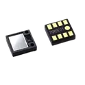
The PAT9125EL-TKIT from PixArt Imaging Inc. is a low-power optical tracking miniature chip designed for precise motion detection using laser-based optical navigation technology. It integrates both the optical sensor and VCSEL laser light source into a single compact package, enabling accurate tracking even on smooth or glossy surfaces. This device captures sequential surface images and processes them internally to determine movement direction, speed, and displacement (X/Y data), which can be accessed by a host controller via digital interfaces. It is particularly suited for space-constrained, battery-powered, and enclosed systems, eliminating the need for mechanical components like code wheels or special surface markings. Key Features Integrated optical sensor + VCSEL laser (850 nm) in a single package No external lens required, simplifying design Wide depth of field (DOF): 1–30 mm, even on reflective surfaces Programmable resolution up to ~1275 CPI Supports I²C (TKIT) interface (SPI variant available as TKMT) Motion detection interrupt output Built-in oscillator (no external clock needed) Low power consumption: Run: ~0.7 mA Sleep: down to 10 µA Power-down: ~5 µA Pre-calibrated laser (no calibration required) IEC/EN 60825-1 Class 1 eye-safe laser compliant Key Specifications Supply Voltage: VDD: 1.7–3.6 V VLD (laser): 2.7–3.6 V Max Tracking Speed: up to ~30 inches/sec Package: 8-pin LGA (3.5 × 3.2 × 1.0 mm) Interface: I²C (for TKIT variant)
3 Uses0 StarsESP32-WROOM-32UE-N16
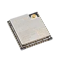
2.4GHz -98dBm SMD,19.2x18mm RF Transceiver Modules and Modems RoHS The ESP32-WROOM-32UE-N16 is a 2.4 GHz wireless MCU module built around the ESP32 SoC. It combines a dual-core processor, integrated Wi-Fi (802.11 b/g/n) and Bluetooth 4.2 (Classic + BLE), along with rich peripherals. The “UE” variant specifically uses a U.FL / IPEX connector for an external antenna, making it ideal for applications that require better RF performance or flexible antenna placement (e.g., enclosed products or long-range communication). The “N16” indicates 16 MB external flash memory, suitable for large firmware, OTA updates, and data-heavy applications. Processing Dual-core Xtensa LX6 32-bit CPU Clock speed up to 240 MHz Memory 16 MB Flash (N16 variant) ~520 KB SRAM + 448 KB ROM Connectivity Wi-Fi: 802.11 b/g/n (up to 150 Mbps) Bluetooth: v4.2 (BR/EDR + BLE) Frequency: 2.4 GHz band Antenna External antenna via U.FL connector Better range and flexibility vs PCB antenna Interfaces / Peripherals GPIO (≈26 usable pins) UART, SPI, I2C, I2S, SDIO ADC, DAC PWM (LED & motor control) Capacitive touch sensing Security Hardware encryption: AES, SHA, RSA Secure boot & flash encryption support Power Operating voltage: 3.0V – 3.6V (typ. 3.3V) Multiple low-power modes for battery applications Environmental Operating temperature: -40°C to +85°C Physical Surface-mount module (~38 pins / 52 pads depending on reference) Compact and RF-shielded design Typical Applications Smart home devices (IoT) Industrial automation Wireless sensors and data loggers Wearables and consumer electronics Remote monitoring systems #Module #ESP32
48 Uses0 StarsESP32-S3-WROOM-1-N8R2
WiFi 802.11a/b/g/n, Bluetooth v5.0 Transceiver Module 2.4GHz PCB Trace The ESP32-S3-WROOM-1-N8R2 is a compact, low-power Wi-Fi and Bluetooth® Low Energy (BLE) module developed by Espressif Systems. It is based on the ESP32-S3 system-on-chip (SoC), which integrates a dual-core Xtensa® LX7 processor optimized for high performance and edge AI processing. This module includes 8 MB of external SPI flash memory and 2 MB of PSRAM, enabling efficient handling of memory-intensive applications such as graphical interfaces, buffering, and embedded machine learning workloads. Designed for flexibility and scalability, the module integrates RF components, power management, and a wide range of peripherals into a surface-mount package suitable for IoT, industrial, and consumer electronics applications. Key Features Dual-core Xtensa® LX7 processor operating up to 240 MHz Integrated 2.4 GHz Wi-Fi (802.11 b/g/n) Bluetooth 5 Low Energy support Embedded 8 MB SPI flash memory Integrated 2 MB PSRAM AI acceleration through vector instruction support USB OTG (full-speed) capability Multiple low-power operating modes Built-in hardware security features Extensive peripheral interface support Functional Overview The module consists of several integrated subsystems, including a dual-core processing unit, memory subsystem (flash and PSRAM), RF subsystem for wireless communication, peripheral interface controllers, power management circuitry, and a hardware-based security engine. Electrical Characteristics Operating voltage range: 3.0 V to 3.6 V (typical 3.3 V) Operating temperature range: -40°C to +85°C RF operating frequency: 2.4 GHz Current consumption varies depending on operating mode, ranging from microamp levels in deep sleep to hundreds of milliamps during active transmission Processor and Memory The module features a dual-core Xtensa® LX7 CPU capable of running at frequencies up to 240 MHz. It includes approximately 512 KB of internal SRAM, supplemented by 8 MB of external flash memory and 2 MB of PSRAM for extended data storage and processing. Wireless Connectivity The ESP32-S3-WROOM-1-N8R2 supports Wi-Fi communication compliant with 802.11 b/g/n standards in the 2.4 GHz band. It also supports Bluetooth 5 Low Energy for short-range wireless communication. The module includes an integrated PCB antenna and supports RF output power up to approximately +20 dBm. Peripheral Interfaces The module provides a wide range of interfaces, including general-purpose input/output (GPIO) pins, SPI, I2C, UART, and I2S for audio applications. It also supports PWM for LED control, a 12-bit analog-to-digital converter (ADC), and USB OTG functionality. Pin functions are multiplexed to maximize flexibility. Power Management Power efficiency is achieved through multiple operating modes, including active mode, modem sleep, light sleep, and deep sleep. The module includes an RTC subsystem for low-power timekeeping and supports dynamic frequency scaling to optimize performance and energy consumption. Security Features The module incorporates several hardware-based security mechanisms, including secure boot, flash encryption, and digital signature verification. It also includes a hardware random number generator and cryptographic accelerators supporting AES, SHA, RSA, and ECC algorithms. Mechanical Characteristics The module is designed for surface-mount integration and measures approximately 18 mm by 25.5 mm. It includes an onboard PCB antenna and is suitable for compact embedded designs. Pin Configuration Overview GPIO pins are multiplexed to support various peripheral functions such as analog inputs, communication interfaces, and control signals. Dedicated pins are provided for power supply, module enable, and boot configuration. Typical Applications Internet of Things (IoT) devices Smart home systems Industrial automation and monitoring Edge AI and machine learning applications Wearable electronics Audio and multimedia systems USB-enabled embedded devices Compliance The module is designed to meet Wi-Fi and Bluetooth standards and is compliant with RoHS requirements. Certification such as FCC or CE may apply depending on the specific module variant and deployment. Ordering Information The ESP32-S3-WROOM-1-N8R2 variant includes 8 MB of flash memory and 2 MB of PSRAM. #commonpartslibrary #integratedcircuit #transceiver #wireless #rf
320 Uses0 StarsADXL355BEZ
Accelerometer X, Y, Z Axis ±2g, 4g, 8g 1.5kHz 14-CLCC (6x6) General Description The ADXL355BEZ is a low noise, low drift, low power, three-axis MEMS accelerometer intended for high-precision sensing applications. It delivers high-resolution digital acceleration data with excellent long-term stability and minimal temperature-induced variation. The device integrates a complete sensing chain, including the MEMS sensor element, analog conditioning, analog-to-digital conversion, and digital filtering. Output data is provided through SPI or I²C interfaces, enabling straightforward integration into embedded and industrial systems. Key Features Three-axis acceleration sensing (X, Y, Z) Selectable full-scale ranges: ±2 g, ±4 g, ±8 g Low noise density (~25 µg/√Hz) Low offset and minimal temperature drift High-resolution 20-bit digital output Integrated digital filtering SPI and I²C communication interfaces Low power consumption (~200 µA typical) Wide supply voltage range (2.25 V to 3.6 V) Integrated temperature sensor Hermetically sealed package Applications Structural health monitoring Vibration measurement and analysis Tilt and inclination sensing Industrial condition monitoring Navigation and inertial systems Seismic detection Robotics and stabilization platforms Functional Description The ADXL355BEZ includes an integrated sensing and processing architecture composed of: Three-axis MEMS sensing element Analog front-end signal conditioning High-resolution ADC Digital filtering and decimation stages Temperature sensing element Digital communication interface (SPI/I²C) Configuration and control registers Electrical Characteristics (Typical) Supply voltage: 2.25 V to 3.6 V Supply current: ~200 µA Output data rate: up to 4 kHz Noise density: ~25 µg/√Hz Resolution: 20-bit Interface: SPI / I²C Mechanical and Package Information Package type: LGA (Land Grid Array) Approximate dimensions: 3 mm × 5 mm × 1 mm Hermetically sealed for improved environmental robustness Interface and Communication Supports SPI (4-wire) and I²C protocols Outputs 20-bit acceleration data per axis Data format: two’s complement Measurement Ranges ±2 g ±4 g ±8 g Environmental Specifications Operating temperature range: -40°C to +125°C Storage temperature range: -55°C to +150°C Power Management Supports measurement and standby modes Designed for low-power operation in continuous sensing applications Compliance and Reliability Industrial-grade device Designed for long-term stability RoHS compliant #commonpartslibrary #sensor #accelerometer
28 Uses0 StarsADXL354BEZ
Accelerometer X, Y, Z Axis ±2g, 4g 1.5kHz 14-CLCC (6x6) General Description The ADXL354BEZ is a low noise, low drift, low power, 3-axis MEMS accelerometer designed for high precision sensing applications. It provides analog voltage outputs proportional to acceleration along the X, Y, and Z axes. The device is optimized for applications requiring high resolution and long-term stability, including structural health monitoring, condition monitoring, tilt sensing, and seismic measurements. The sensor features excellent temperature stability, minimal offset drift, and selectable measurement ranges. Its very low noise density makes it suitable for vibration analysis and other sensitive measurement environments. Key Features 3-axis MEMS accelerometer with analog outputs Selectable measurement ranges of ±2 g, ±4 g, and ±8 g Ultra-low noise density of approximately 20 µg/√Hz Low offset drift across temperature Low power consumption of approximately 150 µA (typical) High resolution and measurement stability Integrated temperature sensor output Hermetically sealed package for improved environmental robustness Functional Description The ADXL354BEZ measures acceleration using capacitive MEMS sensing elements arranged along three orthogonal axes. When acceleration is applied, the internal sensing structure experiences displacement, causing a change in capacitance. This change is converted into an analog voltage output for each axis. Each axis produces a continuous-time analog signal, allowing direct interfacing with external analog-to-digital converters or signal conditioning circuits. Internal signal conditioning ensures low noise performance and stable output behavior. Electrical Characteristics (Typical) The device operates with a supply voltage ranging from 2.25 V to 3.6 V. Typical supply current during normal operation is approximately 150 µA. The noise density for all three axes is around 20 µg/√Hz. The bandwidth is user selectable and can reach up to approximately 1.5 kHz. The output signals are analog and ratiometric with respect to the supply voltage. Mechanical Characteristics The ADXL354BEZ is housed in a compact leadless chip carrier (LCC) package with approximate dimensions of 5 mm by 5 mm. It is designed for surface-mount installation. The sensing axes are aligned orthogonally to provide accurate three-dimensional acceleration measurement. Performance Characteristics High resolution suitable for precision sensing applications Low temperature coefficient and minimal drift over time High linearity across the full-scale measurement range Excellent long-term stability Low cross-axis sensitivity for improved accuracy Pin Configuration Overview The device includes power supply and ground connections, along with individual analog outputs for each axis labeled XOUT, YOUT, and ZOUT. A self-test pin is provided for functionality verification, and a temperature output pin allows monitoring of internal device temperature. Operating Conditions The device is designed to operate over a temperature range from −40°C to +125°C. Storage temperature ranges from −65°C to +150°C. The recommended supply voltage range is 2.25 V to 3.6 V. Applications Structural health monitoring Industrial condition monitoring Seismic and geophysical sensing Tilt and inclination measurement Platform stabilization systems Vibration analysis Advantages Extremely low noise performance for high sensitivity applications Stable operation across wide temperature ranges Simple analog interface without the need for digital communication protocols Robust packaging suitable for harsh environments Compliance and Reliability The ADXL354BEZ is RoHS compliant and designed for industrial-grade applications. It offers high reliability and long-term performance stability in demanding operating conditions. #commonpartslibrary #sensor #accelerometer
3 Uses0 StarsADXL335BCPZ-RL7
Accelerometer X, Y, Z Axis ±3g 1.6kHz (X,Y), 550Hz (Z) 16-LFCSP-LQ (4x4) The ADXL335BCPZ-RL7 is a low-power, complete 3-axis accelerometer with analog voltage outputs proportional to acceleration. It measures acceleration along the X, Y, and Z axes with a full-scale range of ±3 g. This device integrates a micro-electromechanical system (MEMS) sensor with signal conditioning circuitry, enabling direct analog output without the need for external amplification. The RL7 suffix indicates tape-and-reel packaging for automated assembly. The ADXL335BCPZ-RL7 is designed for compact, battery-powered, and motion-sensitive applications where low power consumption and ease of integration are critical. Functional Overview The accelerometer operates using a capacitive sensing structure. Acceleration causes displacement of an internal mass, changing capacitance, which is converted into a proportional analog voltage output. Each axis operates independently and provides a continuous analog signal that can be read by a microcontroller’s ADC. External capacitors allow the user to configure bandwidth per axis, enabling optimization for noise or response speed. Electrical Characteristics Supply Voltage Range: 1.8 V to 3.6 V Supply Current: Typical: 350 µA Measurement Range: ±3 g Sensitivity (Typical): 300 mV/g Zero-g Bias Level: Approximately VCC / 2 Bandwidth: Adjustable via external capacitors Typical limits: X, Y axes: up to 1600 Hz Z axis: up to 550 Hz Output Characteristics Output Type: Analog (ratiometric to supply voltage) Axes: Three independent outputs (XOUT, YOUT, ZOUT) Output Impedance: Approximately 32 kΩ Noise Density: X/Y axes: ~150 µg/√Hz Z axis: ~300 µg/√Hz Mechanical Characteristics Package Type: 16-lead LFCSP Package Dimensions: Approximately 4 mm × 4 mm × 1.45 mm Mounting: Surface mount Packaging Option: Tape and reel (RL7) Environmental Specifications Operating Temperature Range: −40°C to +85°C Storage Temperature Range: −65°C to +150°C Shock Survival: Up to 10,000 g Interface Requirements External Components: Capacitors required for bandwidth selection (one per axis) Interface Type: Analog voltage outputs compatible with ADC inputs Pin Description (Summary) ST: Self-test input XOUT: X-axis analog output YOUT: Y-axis analog output ZOUT: Z-axis analog output VCC: Power supply GND: Ground NC: No connection / reserved Applications Tilt and orientation sensing Motion and vibration detection Portable electronics Gaming controllers Wearable devices Industrial monitoring systems Key Features Three-axis acceleration measurement Low power consumption Analog output for simple interfacing Compact MEMS package Adjustable bandwidth Wide temperature operating range Tape-and-reel packaging for automated manufacturing #commonpartslibrary #integratedcircuit #sensor #accelerometer
2 Uses0 Stars