Interface ICs
An interface IC is a type of integrated circuit that is designed to facilitate communication between two devices or systems. These devices are commonly used in electronic systems to enable the transfer of data and control signals between different components or subsystems. Some common use cases for interface ICs include connecting microcontrollers to peripherals such as sensors or displays, linking multiple processors together in a network, and enabling communication between devices using different communication protocols. Flux.ai has the world's largest community-driven public library of interface ICs, with footprints, symbols, datasheets, and simulation models. This library is a valuable resource for engineers and designers who need access to accurate and up-to-date information on these important components. Whether you are working on a new design project or simply looking to learn more about interface ICs, Flux.ai is an excellent resource to help you find the information you need.
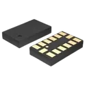
LIS2MDLTR
Magnetic Sensors LIS2MDLTR LGA-12_L2.0-W2.0-P0.50-BL LCSC Part Number: C919695 JLCPCB Part Class: Extended Part Manufactured by ST(意法半导体) STMicroelectronics LIS2MDL ultralow-power high-performance 3-axis digital magnetometer, ±50 gauss magnetic dynamic range, 16-bit data output, SPI and I2C serial interfaces, 1.71V to 3.6V analog supply voltage, selectable power modes and resolution, single measurement mode, programmable interrupt generator, embedded self-test and temperature sensor, -40°C to +85°C operating range, LGA-12 package 2.0 x 2.0 x 0.7mm. Search Keywords: LIS2MDL, LIS2MDLTR, ST LIS2MDL, STMicroelectronics LIS2MDL, LIS2MDL magnetometer, 3-axis magnetometer, digital magnetic sensor, 3-axis digital magnetic sensor, ±50 gauss magnetometer, I2C SPI magnetometer, 16-bit magnetometer, low power magnetometer, compass sensor, LGA-12 magnetometer, 2x2mm magnetometer Hashtags: #LIS2MDL #LIS2MDLTR #STMicroelectronics #Magnetometer #3AxisMagnetometer #DigitalMagneticSensor #CompassSensor #I2CSensor #SPISensor #16BitSensor #LowPowerSensor #50GaussSensor #LGA12
24 Uses0 StarsQMC5883L
Magnetic Sensors QMC5883L LGA-16_L3.0-W3.0-P0.50-BL_SQ The QMC5883L is a multi-chip three-axis magnetic sensor. This surface -mount, small sized chip has integrated magnetic sensors with signal condition ASIC, targeted for high precision applications such as compassing, navigation and gaming in drone, robot, mobile and personal hand-held devices. The QMC5883L is based on our state-of-the-art, high resolution, magneto-resistive technology licensed from Honeywell AMR technology. Along with custom-designed 16-bit ADC ASIC, it offers the advantages of low noise, high accuracy, low power consumption, offset cancellation and temperature compensation. QMC5883L enables 1° to 2° compass heading accuracy. The I²C serial bus allows for easy interface. The QMC5883L is in a 3x3x0.9mm3 surface mount 16-pin land grid array (LGA) package. 3-Axis Magneto-Resistive Sensors in a 3x3x0.9 mm3 Land Grid Array Package (LGA), guaranteed to operate over an extended temperature range of -40 °C to +85 °C. Small Size for Highly Integrated Products. Signals Have Been Digitized And Calibrated. 16 Bit ADC With Low Noise AMR Sensors Achieves 2 Milli-Gauss Field Resolution Enables 1° To 2° Degree Compass Heading Accuracy , Allows for Navigation and LBS Applications Wide Magnetic Field Range (±8 Gauss) Maximizes Sensor’s Full Dynamic Range and Resolution Temperature Compensated Data Output and Temperature Output Automatically Maintains Sensor’s Sensitivity Under Wide Operating Temperature Range I 2C Interface with Standard and Fast Modes. High-Speed Interfaces for Fast Data Communications. Maximum 200Hz Data Output Rate Wide Range Operation Voltage (2.16V To 3.6V) and Low Power Consumption (75A) Compatible with Battery Powered Applications Lead Free Package Construction RoHS Compliance Software And Algorithm Support Available Compassing Heading, Hard Iron, Soft Iron, and Auto Calibration Libraries Available #CommonPartsLibrary #Sensor
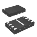
59 Uses0 StarsW25Q16JVUXIQ
SPI Flash Serial Flash Memory with Dual/Quad SPI The W25Q16JVUXIQ is a 16-Mbit (2-MByte) Serial NOR Flash memory device from Winbond. It is designed for embedded systems that require non-volatile code and data storage with minimal pin count, low power consumption, and high-speed access. The device supports standard SPI, Dual SPI, and Quad SPI interfaces, making it suitable for firmware storage, boot memory, IoT devices, microcontrollers, consumer electronics, and execute-in-place (XIP) applications. Key Features 16-Mbit (2-MByte) Flash Memory Capacity Operating Voltage: 2.7 V to 3.6 V Standard SPI, Dual SPI, and Quad SPI Interface Support Maximum SPI Clock Frequency: 133 MHz Equivalent Data Transfer Rates: 266 MHz (Dual SPI) 532 MHz (Quad SPI) Continuous Read and XIP (Execute-In-Place) Capability 4 KB Sector Erase, 32 KB Block Erase, 64 KB Block Erase, and Chip Erase 256-Byte Programmable Page Size Minimum 100,000 Program/Erase Cycles per Sector More Than 20 Years Data Retention Ultra-Low Power Consumption Typical power-down current below 1 µA 64-Bit Unique Serial Number Three 256-Byte Security Registers with OTP Protection JEDEC ID and SFDP Support Software and Hardware Write Protection Operating Temperature Options up to +85°C and +105°C Compact 8-Pad USON Package (2 mm × 3 mm) suitable for space-constrained designs #CommonPartsLibrary #IntegratedCircuit #Memory
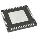
184 Uses0 StarsESP32-S3FH4R2
2.4GHz Wi-Fi+Bluetooth LE SoC ESP32-S3FH4R2 is a highly integrated low-power Wi-Fi and Bluetooth LE System-on-Chip (SoC) from Espressif Systems. It is based on a dual-core Xtensa® LX7 processor running at up to 240 MHz and is designed for IoT, smart home, industrial control, AIoT, audio processing, and embedded applications. The ESP32-S3FH4R2 variant includes 4 MB of in-package Quad SPI Flash and 2 MB of in-package Quad SPI PSRAM, reducing external component count and simplifying PCB design. Key Features Dual-core Xtensa® LX7 CPU Up to 240 MHz operating frequency 32-bit architecture with floating-point unit (FPU) SIMD instructions for AI and signal-processing workloads Integrated Memory 4 MB in-package Flash 2 MB in-package PSRAM 512 KB on-chip SRAM 384 KB ROM Additional RTC memory for low-power operation Wireless Connectivity IEEE 802.11 b/g/n 2.4 GHz Wi-Fi Bluetooth® 5 Low Energy (LE) Long-range and low-power wireless communication support Rich Peripheral Set Up to 45 programmable GPIOs USB OTG and USB Serial/JTAG SPI, I²C, I²S, UART, SDIO TWAI® (CAN 2.0 compatible) Camera interface LCD interface PWM, pulse counter, RMT, DMA controller Analog Features Two 12-bit SAR ADCs Temperature sensor 14 capacitive touch sensing inputs Security Features Secure Boot Flash Encryption AES, SHA, RSA, HMAC hardware accelerators True Random Number Generator (RNG) Digital Signature peripheral Low-Power Operation Multiple power-saving modes ULP-RISC-V coprocessor ULP-FSM coprocessor Deep-sleep support with RTC memory retention
28 Uses0 StarsLAN8720A-CP-TR-ABC
Small Footprint RMII 10/100 Ethernet Transceiver with HP Auto-MDIX Support LAN8720A-CP-TR-ABC is a low-power, single-port 10BASE-T/100BASE-TX Ethernet Physical Layer (PHY) transceiver from Microchip Technology. It is designed to connect a microcontroller, processor, or Ethernet MAC to a standard Ethernet network through an RMII (Reduced Media Independent Interface). The device is widely used in embedded networking applications such as industrial controllers, IoT gateways, IP cameras, networked printers, routers, and ESP32-based Ethernet designs. Key Features Single-chip 10/100 Mbps Ethernet PHY Supports both 10BASE-T and 100BASE-TX Ethernet operation. RMII Interface Reduced pin-count interface for easy connection to Ethernet MACs and microcontrollers. IEEE 802.3 / 802.3u Compliant Fully compliant with Fast Ethernet standards. HP Auto-MDIX Support Automatically detects and configures straight-through or crossover Ethernet cables. Auto-Negotiation Automatically selects the best available speed and duplex mode. Flexible I/O Voltage Supports LVCMOS I/O voltages from 1.6 V to 3.6 V, simplifying interfacing with different processors. Integrated 1.2 V Regulator Allows operation from a single 3.3 V supply, reducing external components. Low-Power Architecture Features multiple power-saving modes through Microchip's flexPWR® technology. Built-in Diagnostics and Reliability Features Loopback modes, automatic polarity correction, link-status monitoring, and wake-up detection. Compact Package Available in a 24-pin SQFN/QFN (4 mm × 4 mm) package for space-constrained designs #CommonPartsLibrary #IntegratedCircuit
95 Uses0 Stars91302-67-067R2M
M.2 CONN.P=0.5 6.7mm H conn The 91302-67-067R2M is a 67-position M.2 (NGFF) card-edge connector manufactured by UMAX. It is designed for connecting M.2 SSDs and PCIe-based expansion modules to a host PCB. The connector features an M-Key interface, making it suitable for high-speed PCIe storage applications such as NVMe solid-state drives. It is a surface-mount, right-angle receptacle with a 0.5 mm contact pitch and a 6.7 mm height above the PCB. Key Features M.2 M-Key connector Supports M-Key M.2 modules, commonly used for PCIe/NVMe SSDs. 67 contacts (67P) Standard pin count for M-Key M.2 card-edge connections. 0.5 mm pitch Fine-pitch design suitable for compact, high-density PCB layouts. Surface-mount, right-angle mounting Optimized for automated PCB assembly and low-profile system designs. 6.7 mm connector height Provides compatibility with standard M.2 card installation requirements. Female card-edge receptacle Accepts M.2 modules directly without additional adapters. RoHS compliant Meets environmental requirements for lead-free electronic assemblies. Typical Applications NVMe SSD sockets PCIe M.2 storage devices Embedded computing systems Industrial PCs Networking equipment Edge AI and IoT gateways Single-board computers requiring M.2 expansion #CommonPartsLibrary #Connector
160 Uses0 StarsADXL345TCCZ-EP
Accelerometer X, Y, Z Axis ±2g, 4g, 8g, 16g 0.05Hz ~ 1.6kHz 14-LGA (3x5) The ADXL345-EP is an extended performance version of the ADXL345, which is a small, thin, ultralow power, 3-axis accelerometer with high resolution (13-bit) measurement at up to ±16 g. Digital output data is formatted as 16-bit twos complement and is accessible through either a SPI (3- or 4-wire) or I2 C digital interface. The ADXL345-EP is well suited for extended temperature range industrial and aerospace equipment. It measures the static acceleration of gravity in tilt-sensing applications, as well as dynamic acceleration resulting from motion or shock. Its high resolution (3.9 mg/LSB) enables measurement of inclination changes less than 1.0°. Several special sensing functions are provided. Activity and inactivity sensing detect the presence or lack of motion by comparing the acceleration on any axis with user-set thresholds. Tap sensing detects single and double taps in any direction. Freefall sensing detects if the device is falling. These functions can be mapped individually to either of two interrupt output pins. An integrated memory management system with a 32-level first in, first out (FIFO) buffer can be used to store data to minimize host processor activity and lower overall system power consumption. Low power modes enable intelligent motion-based power management with threshold sensing and active acceleration measurement at extremely low power dissipation. The ADXL345-EP is supplied in a small, thin, 3 mm × 5 mm × 1 mm, 14-lead, enhanced plastic package. Ultralow power: as low as 23 µA in measurement mode and 0.1 µA in standby mode at VS = 2.5 V (typical) Power consumption scales automatically with bandwidth User-selectable resolution from 10 to 13 bits 4 mg/LSB scale factor in all g ranges 32-sample FIFO minimizes host processor load Single tap, double tap, and free-fall detection Activity/inactivity monitoring Supply voltage range: 2.0 V to 3.6 V I/O voltage range: 1.7 V to VS SPI (3- and 4-wire) and I2C digital interfaces Flexible interrupt modes mappable to either interrupt pin Measurement ranges selectable via serial command Bandwidth selectable via serial command 10,000 g shock survival Pb free/RoHS compliant Small and thin: 3 mm × 5 mm × 1 mm LGA package #CommonPartsLibrary #Sensor #Motion-sensor #accelerometer
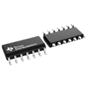
49 Uses0 StarsSN74HCT125DRE4
Buffers / Drivers SN74HCT125DRE4 SOIC-14_L8.6-W3.9-P1.27-LS6.0-BL LCSC Part Number: C2675588 JLCPCB Part Class: Extended Part Manufactured by TI(德州仪器) Texas Instruments SN74HCT125/SN54HCT125 quadruple bus buffer IC with 3-state outputs, contains four independent non-inverting buffers with TTL-compatible inputs, positive logic function Y=A, 4.5V to 5.5V operating voltage range, high-current outputs capable of driving up to 15 LSTTL loads, ±6mA output drive at 5V, low input current, typical 12ns propagation delay, suitable for bus line driving, memory address buffering and digital logic interface applications, available in SOIC-14 and PDIP-14 packages. Search Keywords: SN74HCT125, SN54HCT125, Texas Instruments SN74HCT125, TI SN74HCT125, SN74HCT125 buffer, 74HCT125 buffer, quad bus buffer, quadruple bus buffer, 3-state buffer IC, tri-state buffer IC, non-inverting buffer IC, TTL-compatible CMOS buffer, HCT logic buffer, bus line driver, memory address buffer, SN74HCT125D, SN74HCT125N, SOIC-14 buffer, PDIP-14 buffer, SN74HCT125 datasheet Hashtags: #SN74HCT125 #SN54HCT125 #74HCT125 #TexasInstrumentsSN74HCT125 #TIBufferIC #BusBuffer #QuadBusBuffer #TriStateBuffer #3StateBuffer #NonInvertingBuffer #HCTLogic #TTLCompatibleInput #LogicBufferIC #BusLineDriver #AddressBuffer #SOIC14 #PDIP14
31 Uses0 Stars