Interface ICs
An interface IC is a type of integrated circuit that is designed to facilitate communication between two devices or systems. These devices are commonly used in electronic systems to enable the transfer of data and control signals between different components or subsystems. Some common use cases for interface ICs include connecting microcontrollers to peripherals such as sensors or displays, linking multiple processors together in a network, and enabling communication between devices using different communication protocols. Flux.ai has the world's largest community-driven public library of interface ICs, with footprints, symbols, datasheets, and simulation models. This library is a valuable resource for engineers and designers who need access to accurate and up-to-date information on these important components. Whether you are working on a new design project or simply looking to learn more about interface ICs, Flux.ai is an excellent resource to help you find the information you need.
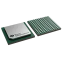
ADC09SJ1300AAVT
Analog to Digital Converters - ADC Single-channel, 9-bit, 1.3-GSPS analog-to-digital converter (ADC) with JESD204C interface 144-FCBGA -40 to 85 ADC09xJ1300 is a family of quad, dual and single channel, 9-bit, 1.3GSPS analog-to-digital converters (ADC). Low power consumption, high sampling rate and 9-bit resolution makes the ADC09xJ1300 ideally suited for suited for a variety of multi-channel communications and test systems. Full-power input bandwidth (-3dB) of 6GHz enables direct RF sampling of L-band and S-band. A number of clocking features are included to relax system hardware requirements, such as an internal phase-locked loop (PLL) with integrated voltagecontrolled oscillator (VCO) to generate the sampling clock. Four clock outputs are provided to clock the logic and SerDes of the FPGA or ASIC. A timestamp input and output is provided for pulsed systems. JESD204C serialized interface decreases system size by reducing the amount of printed circuit board (PCB) routing. Interface modes support from 2 to 8 lanes (dual and quad channel devices) or 1 to 4 lanes (for the single channel device), with SerDes baud-rates up to 17.16Gbps, to allow the optimal configuration for each application. Features • ADC Core: – Resolution: 9 Bit – Maximum sampling rate: 1.3GSPS – Non-interleaved architecture – Internal dither reduces high-order harmonics • Performance specifications (–1dBFS): – SNR (100 MHz): 53.5dBFS – ENOB (100 MHz): 8.5 Bits – SFDR (100 MHz): 64dBc – Noise floor (–20dBFS): –143dBFS • Full-scale input voltage: 80 mVPP-DIFF • Full-power input bandwidth: 6GHz • JESD204C Serial data interface: – Support for 2 to 8 (Quad/Dual channel) or 1 to 4 (Single channel) total SerDes lanes – Maximum baud-rate: 17.16Gbps – 64B/66B and 8B/10B encoding modes – Subclass-1 support for deterministic latency – Compatible with JESD204B receivers • Optional internal sampling clock generation – Internal PLL and VCO (7.2–8.2GHz) • SYSREF Windowing eases synchronization • Four clock outputs simplify system clocking – Reference clocks for FPGA or adjacent ADC – Reference clock for SerDes transceivers • Timestamp input and output for pulsed systems • Power consumption (1GSPS): – Quad Channel: 450mW / channel – Dual channel: 625mW / channel – Single channel: 940mW • Power supplies: 1.1V, 1.9V #CommonPartsLibrary #IntegratedCircuit #ADC #HighSpeedADC #RFADC #JESD204C #13GSPS #9bitADC #DirectRFSampling #TexasInstruments #MixedSignal #DataAcquisition #JESD204
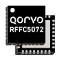
0 Uses0 StarsRFFC5072
The RFFC5072 is a highly integrated wideband RF frequency conversion IC that combines a fractional-N PLL synthesizer, low phase-noise VCO, and a high-linearity RF mixer in a single device. It is designed for wireless infrastructure, software-defined radio (SDR), test equipment, military communications, and broadband frequency conversion applications. The device can generate local oscillator (LO) frequencies from 85 MHz to 4.2 GHz and perform frequency conversion for RF signals up to 6 GHz while maintaining excellent phase noise and spurious performance. Features 85MHz to 4200MHz LO Frequency Range Fractional-N Synthesizer with Very Low Spurious Levels Typical Step Size 1.5Hz Fully Integrated Low Phase Noise VCO and LO Buffers Integrated Phase Noise • 0.18° rms at 1GHz • 0.50° rms at 3GHz High Linearity RF Mixer(s) 30MHz to 6000MHz Mixer Frequency Range Input IP3 +23dBm Mixer Bias Adjustable for Low Power Operation Full Duplex Mode (RFFC5071) 2.7V to 3.3V Power Supply Low Current Consumption 3- or 4-Wire Serial Interface Applications Wideband Radios Distributed Antenna Systems Diversity Receivers Software Defined Radios Frequency Band Shifters Point-to-Point Radios WiMax/LTE Infrastructure Satellite Communications Wideband Jammers #RFFC5072 #Qorvo #RFMixer #FrequencySynthesizer #PLL #VCO #WidebandRF #FrequencyConverter #SDR #WirelessInfrastructure #RFDesign #MicrowaveEngineering #Telecommunications #EmbeddedSystems #ElectronicsDesign #RFIC #SignalProcessing #HardwareEngineering
4 Uses0 StarsOPT4060DTSR
Texas Instruments OPT4060 high-speed high-sensitivity RGBW color sensor, single-chip light-to-digital sensor with four optical channels for red, green, blue and wide/clear band measurement, I2C interface, semi-logarithmic output with wide dynamic range from 2.15mlux to 144klux, 12 configurable conversion times from 600µs to 800ms, automatic full-scale light range selection, selectable I2C address, interrupt output, low 24µA operating current and 2µA standby current, 1.6V to 3.6V supply range, 5.5V tolerant I/Os, SOT-5X3 2.1 x 1.9 x 0.6mm package. Search Keywords: OPT4060, Texas Instruments OPT4060, TI OPT4060, OPT4060 color sensor, RGBW color sensor, high speed color sensor, high sensitivity color sensor, I2C color sensor, light to digital sensor, RGB light sensor, ambient light color sensor, wide dynamic range light sensor, 144klux sensor, SOT-5X3 color sensor, OPT4060 Hashtags: #OPT4060 #TexasInstrumentsOPT4060 #TIColorSensor #RGBWSensor #ColorSensor #LightSensor #LightToDigitalSensor #I2CSensor #AmbientLightSensor #HighSensitivitySensor #HighSpeedSensor #144kluxSensor #SOT5X3
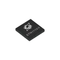
0 Uses0 StarsSTN1110-I/MM
STN1110-IMM General Description The STN1110-IMM is a multiprotocol OBD-II to UART interpreter integrated circuit designed for automotive diagnostic, telematics, and vehicle communication applications. The device translates OBD-II network traffic into a UART serial data stream for communication with external microcontrollers, embedded processors, and host systems. It supports all legislated OBD-II protocols and provides compatibility with ELM327-based software while offering enhanced processing performance, expanded memory resources, advanced message filtering, firmware upgrade capability, and low-power operation. The device is intended for use in automotive diagnostic tools, fleet management systems, vehicle monitoring equipment, data acquisition systems, and embedded automotive communication products. Engineering Specification Part Number: STN1110-IMM Component Type: OBD-II to UART Interpreter Integrated Circuit Device Category: Automotive Communication Interface IC Package Type: QFN Mounting Type: Surface Mount Device (SMD) Interface Type: * UART * OBD-II Supported Protocols: * ISO 15765-4 CAN * ISO 14230-4 KWP2000 * ISO 9141-2 * SAE J1850 PWM * SAE J1850 VPW Key Features: * Multiprotocol OBD-II support * ELM327 command compatibility * Enhanced ST command extensions * High-speed UART communication * Advanced message filtering * Firmware upgrade capability * Large message buffering * Low-power operation * Automotive diagnostic interface functionality Applications: * OBD-II Scan Tools * Vehicle Diagnostics * Automotive Telematics * Fleet Management Systems * Data Logging Equipment * Embedded Automotive Controllers * Emissions Monitoring Systems * Vehicle Communication Gateways Tags #commonpartslibrary #integratedcircuit #ic #automotive #automotiveelectronics #automotivediagnostics #obdii #obd #uart #vehiclecommunication #telematics #embeddedsystems #communicationinterface #diagnosticinterface #scantool #canbus #kwp2000 #saej1850 #iso9141 #surfaceMount #smd #qfn #electroniccomponent #semiconductor #vehicleelectronics #microcontrollerinterface #datalogging #fleetmanagement #embeddedhardware #hardwaredesign
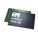
4 Uses0 StarsIM8G32L4JCBG-046I
SDRAM - Mobile LPDDR4X Memory IC 8Gbit Parallel 2.133 GHz 200-FBGA (10x15) The IM8G32L4JCBG-046I is an 8Gb (1GB) LPDDR4X SDRAM memory device designed for high-performance, low-power embedded applications. Organized as 256M × 32 bits, it delivers data rates up to 4266 MT/s, making it suitable for industrial computing, AI edge devices, networking equipment, automotive systems, and other memory-intensive applications. The LPDDR4X architecture reduces power consumption while maintaining high bandwidth and reliable operation across industrial temperature ranges. Key Features 8Gb (Gigabit) LPDDR4X SDRAM Memory organization: 256M × 32 bits High-speed operation up to 4266 MT/s Low-power LPDDR4X interface for reduced energy consumption 32-bit data bus width Industrial operating temperature range: –40°C to +95°C 200-ball FBGA package (10 mm × 15 mm) High bandwidth for demanding embedded applications Optimized for low-power and thermally constrained designs Suitable for industrial, automotive, networking, and edge AI systems #LPDDR4X #SDRAM #MemoryIC #EmbeddedSystems #IndustrialElectronics #EdgeComputing #AIoT #HighSpeedMemory #LowPowerDesign #AutomotiveElectronics #NetworkingHardware #FBGA #HardwareDesign #ElectronicsEngineering #PCBDesign #IntelligentMemory
151 Uses0 Starsrk3566
BGA-565(15.5x14.4) Microcontrollers, Quad-core ARM Cortex-A55 processor The RK3566 is a high-performance, low-power 64-bit application processor developed by Rockchip for AIoT, industrial control, smart displays, tablets, embedded systems, and single-board computers. It integrates a quad-core ARM Cortex-A55 CPU, Mali-G52 GPU, AI acceleration engine (NPU), advanced multimedia processing, and a rich set of connectivity interfaces, making it suitable for Linux- and Android-based applications requiring efficient performance and multimedia capabilities. Key Features Quad-core 64-bit ARM Cortex-A55 processor operating up to 2.0 GHz. ARM Mali-G52 2EE GPU with support for OpenGL ES 3.2, OpenCL 2.0, and Vulkan 1.1. Integrated NPU delivering up to 1 TOPS AI computing performance. Supports DDR3, DDR3L, DDR4, LPDDR3, LPDDR4, and LPDDR4X memory. Hardware video decoding up to 4K@60fps for H.264, H.265, and VP9 formats. Hardware video encoding up to 1080p@60fps for H.264 and H.265. Built-in 8MP ISP with HDR image processing support. Multiple display interfaces including HDMI 2.0, eDP, MIPI-DSI, LVDS, RGB, and E-Ink. High-speed connectivity with USB 3.0, USB 2.0, PCIe, SATA, Gigabit Ethernet, SDIO, and eMMC 5.1. Rich peripheral support including UART, SPI, I²C, PWM, ADC, I²S, PDM, and GPIO. Optimized for Android, Linux, industrial HMI, smart home, edge computing, and AIoT applications. Manufactured using a 22 nm process for improved power efficiency. #RK3566 #Rockchip #ARMCortexA55 #MaliG52 #AIoT #EmbeddedSystems #SingleBoardComputer #Linux #Android #IndustrialControl #SmartDisplay #EdgeComputing #SoC #Processor #NPU #4KVideo #IoT #Electronics #HardwareDesign #PCBDesign
5 Uses0 Stars